Microlithography projection objective

a technology of microlithography and objective, applied in the direction of microlithography exposure apparatus, printers, instruments, etc., can solve the problems of object leakage, inability to correctly, and ineffective relief, and achieve the effect of improving image properties and effective suppression of stray or false ligh

Inactive Publication Date: 2014-10-02
CARL ZEISS SMT GMBH
View PDF9 Cites 2 Cited by
  • Summary
  • Abstract
  • Description
  • Claims
  • Application Information

AI Technical Summary

Benefits of technology

[0024]It is an object of the present invention to provide a microlithography projection objective of the type mentioned at the beginning whose imaging properties are improved by a more effective suppression of stray or false light.

Problems solved by technology

A problem that can arise in the case of projection objectives with beam deflection is that a portion of the light passing through the projection objective leaks at the beam deflecting device directly from the first objective part into the third objective part by omitting the second objective part.
Such stray light or false light therefore does not traverse all the optical elements of the projection objective and is thus incapable of correctly imaging into the image plane of the projection objective the pattern arranged in the object plane of the projection objective, since the projection objective is designed such that only light that traverses all the optical elements in the prescribed sequence can contribute to proper imaging.
However, this does not effectively alleviate, still less eliminate, the problem of the partial direct light leakage from the first objective part into the third objective part.
A round field would have the effect of being unable to make use of the complete wafer surface and is therefore not used in facilities for the mass production of semiconductors.
Irrespective of the particular cause, false light disturbs the lithographic process as soon as it falls onto the wafer since the structures imaged by the exposure process widen owing to the false light background.
In other words, false light that is propagating in the projection objective and reaches the image plane of the projection objective disturbs the contrast of the imaging of the pattern into the image plane.
False images arise in a projection objective owing to false light that does not traverse all the optically operative surfaces of the projection objective, or that while actually traversing all the optically active surfaces of the projection objective does so in a sequence other than is required for proper imaging.
The false light that contributes to this imaging is certainly weak, since it arises chiefly from a reflection at a refracting surface that mostly also has a layer for reducing reflection.
In any event, false light in projection objectives worsens the imaging properties of the projection objective such that there is a need for projection objectives in which false light is suppressed as effectively as possible.
Still another problem in microlithography projection objectives arises in connection with the requirement to provide a uniform aperture over the entire used field.
In projection objectives for microlithography, a vignetting, as it is known, for example, in objectives for photography, is undesired.
However, there are optical designs in which a single aperture stop cannot guarantee the desired uniform aperture over the used field.
These over-aperture rays are typically strongly aberrated and, when reaching the image plane, disturb the uniformity of the image field.

Method used


Image

  • Microlithography projection objective
  • Microlithography projection objective
  • Microlithography projection objective

Examples


Embodiment Construction

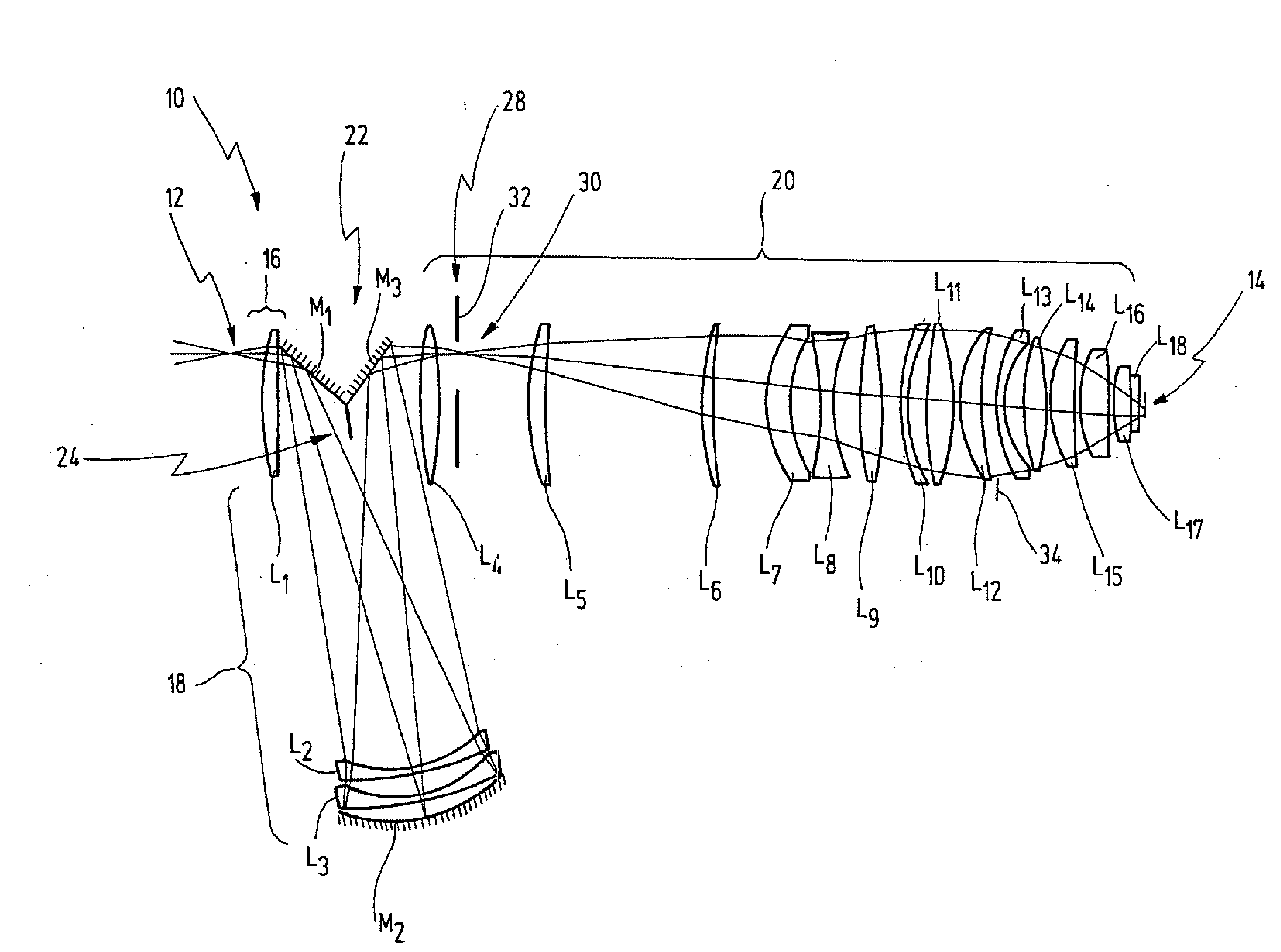
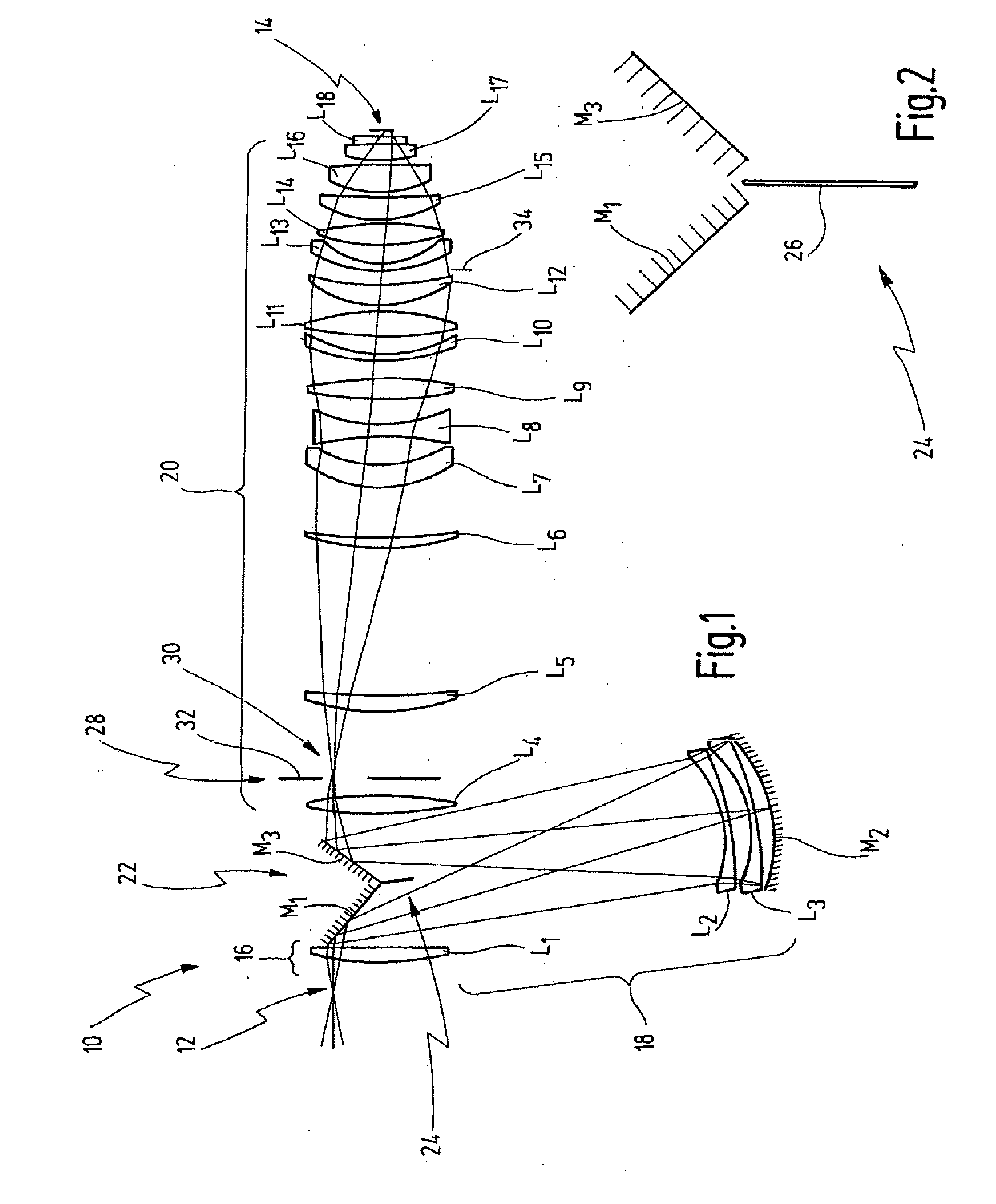
[0106]FIG. 1 shows a microlithography projection objective provided with the general reference numeral 10 intended for imaging into an image plane 14 a pattern (not shown) arranged in an object plane 12.

[0107]The projection objective 10 has a first objective part 16, a second objective part 18 and a third objective part 20.

[0108]The first objective part 16 is dioptric and is formed by a lens L1.

[0109]The second objective part 18 is catadioptric and has lenses L2, L3 and a concave mirror M2.

[0110]The third objective part 20 is dioptric and has lenses L4 to L17 and an end plate L18.

[0111]As shown in FIG. 1, the light propagation direction in the second objective part 18 differs from the light propagation direction in the first objective part 12 and in the third objective part 20. To this end, the projection objective 10 has a beam deflecting device 22, that is formed in the exemplary embodiment shown by two folding mirrors M1 and M3. The folding mirror M1 deflects the light beam comin...


PUM

PropertyMeasurementUnit
angleaaaaaaaaaa
optically activeaaaaaaaaaa
wavelengthaaaaaaaaaa

Abstract

Microlithography projection objectives for imaging into an image plane a pattern arranged in an object plane are described with respect to suppressing false light in such projection objectives.

Description

CROSS-REFERENCE TO RELATED APPLICATIONS[0001]This application is a continuation of, and claims priority under 35 USC 120 to, U.S. application Ser. No. 11 / 916,162, filed May 16, 2008, which is a National Phase application under 35 U.S.C. §371 filed from International Patent Application Serial No. PCT / EP2006 / 004876, filed on May 23, 2006, which claims priority to U.S. Provisional Application Ser. No. 60 / 790,616, filed Apr. 10, 2006, and Ser. No. 60 / 686,784, filed Jun. 2, 2005.BACKGROUND OF THE INVENTION[0002]The invention relates to a microlithography projection objective for imaging into an image plane a pattern arranged in an object plane.[0003]The invention further relates to a projection exposure machine having such a projection objective.[0004]The invention relates, furthermore, to a method for producing semiconductor components and other finely structured subassemblies.[0005]Microlithography projection objectives are used in projection exposure machines for producing semiconduct...

Claims


Application Information

Patent Timeline
Patent Type & Authority Applications(United States)
IPC IPC(8): G03F7/20
CPCG03F7/70225G03F7/70283G03F7/70941G02B17/08G03F7/702
Inventor FELDMANN, HEIKOKRAEHMER, DANIELPERRIN, JEAN-CLAUDEKALLER, JULIANDODOC, AURELIANKAMENOV, VLADIMIRCONRADI, OLAFGRUNER, TORALFOKON, THOMASEPPLE, ALEXANDER
Owner CARL ZEISS SMT GMBH
Why Eureka
Try Eureka