Organic electroluminescent element
an electroluminescent element and organic technology, applied in the field of organic electroluminescent elements, can solve the problems of inability to achieve the practical use of blue phosphorescent materials with good power efficiency, inability to completely eliminate thermal deactivation processes without emission, and inability to achieve the effect of high emission quantum yield
- Summary
- Abstract
- Description
- Claims
- Application Information
AI Technical Summary
Benefits of technology
Problems solved by technology
Method used
Image
Examples
example 1
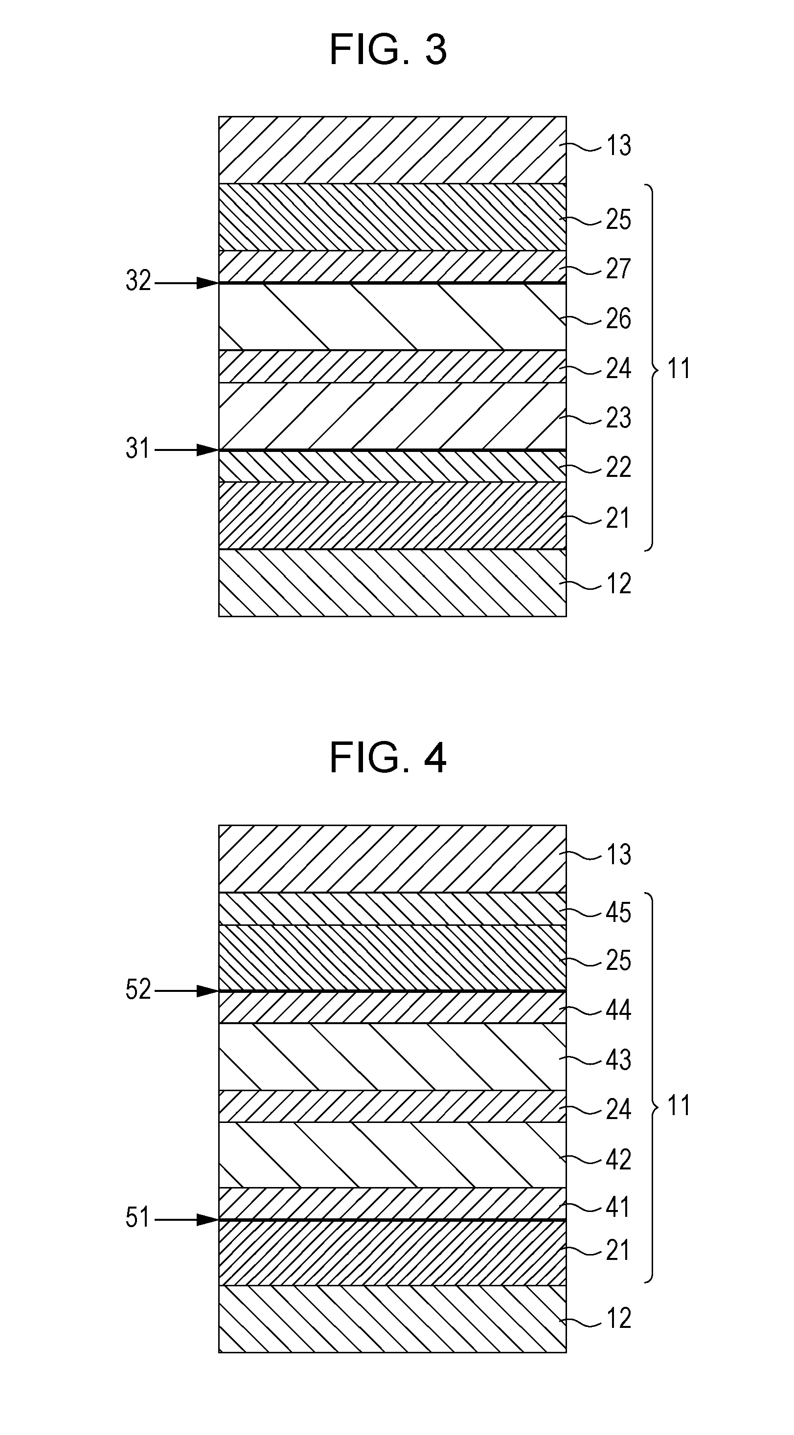
[0045]An organic EL element, having a configuration shown in FIG. 3, including an electron injection sub-layer (not shown) disposed between a cathode 13 and an electron transport sub-layer 25 was prepared by a procedure below.
[0046]A layer of an Ag alloy (Ag—Pd—Cu) used as a reflective metal was formed on a glass substrate serving as a support by a sputtering process so as to have a thickness of about 100 nm and was then patterned. An ITO layer serving as a transparent conductive film was formed on the Ag alloy layer by a sputtering process so as to have a thickness of about 20 nm and was then patterned, whereby an anode 12 serving as a reflective electrode was formed. An isolation film was formed on the anode 12 using an acrylic resin, whereby an anode-bearing substrate was prepared. The anode-bearing substrate was ultrasonically cleaned with isopropyl alcohol (IPA), was boiled in IPA, and was then dried. After the anode-bearing substrate was cleaned with UV light and ozone, an org...
example 2
[0064]An organic EL element was prepared in substantially the same manner as that described in Example 1 except that an exciton inhibition sub-layer with a thickness of 2 nm was formed between a fluorescent light-emitting sub-layer 22 and an exciton generation sub-layer 23 using TAPC.
[0065]In the organic EL element, the LUMO of TAPC of the exciton inhibition sub-layer is 1.86 eV and the LUMO of CBP of the exciton generation sub-layer 23 is 2.54 eV. Therefore, an energy barrier for electrons is present at the interface between the exciton inhibition sub-layer and the exciton generation sub-layer 23. Electrons are accumulated on the exciton generation sub-layer 23 side of the interface and carrier recombination occurred, so that excitons are generated. Some of the accumulated electrons pass through the interface and therefore excitons are generated in a region on the exciton inhibition sub-layer side of the interface. However, this does not lead to the excitation or thermal deactivati...
PUM
 Abstract
Description
Claims
Application Information


