Ion sensitive device and method of fabrication
- Summary
- Abstract
- Description
- Claims
- Application Information
AI Technical Summary
Benefits of technology
Problems solved by technology
Method used
Image

Examples
Embodiment Construction
[0052]It is to be understood that this invention is not limited to particular aspects of the present invention described, as such may, of course, vary. It is also to be understood that the terminology used herein is for the purpose of describing particular aspects only, and is not intended to be limiting, since the scope of the present invention will be limited only by the appended claims.
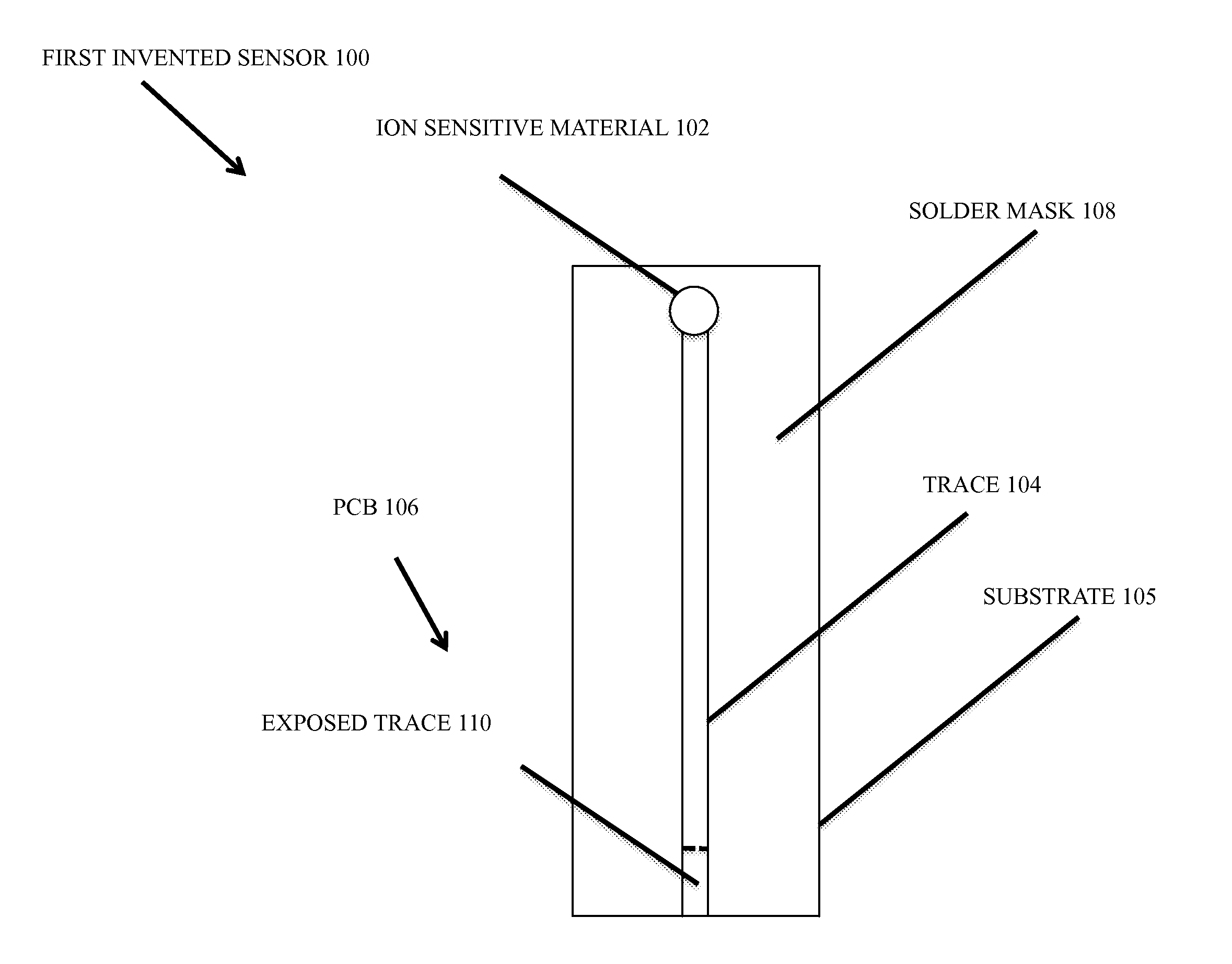
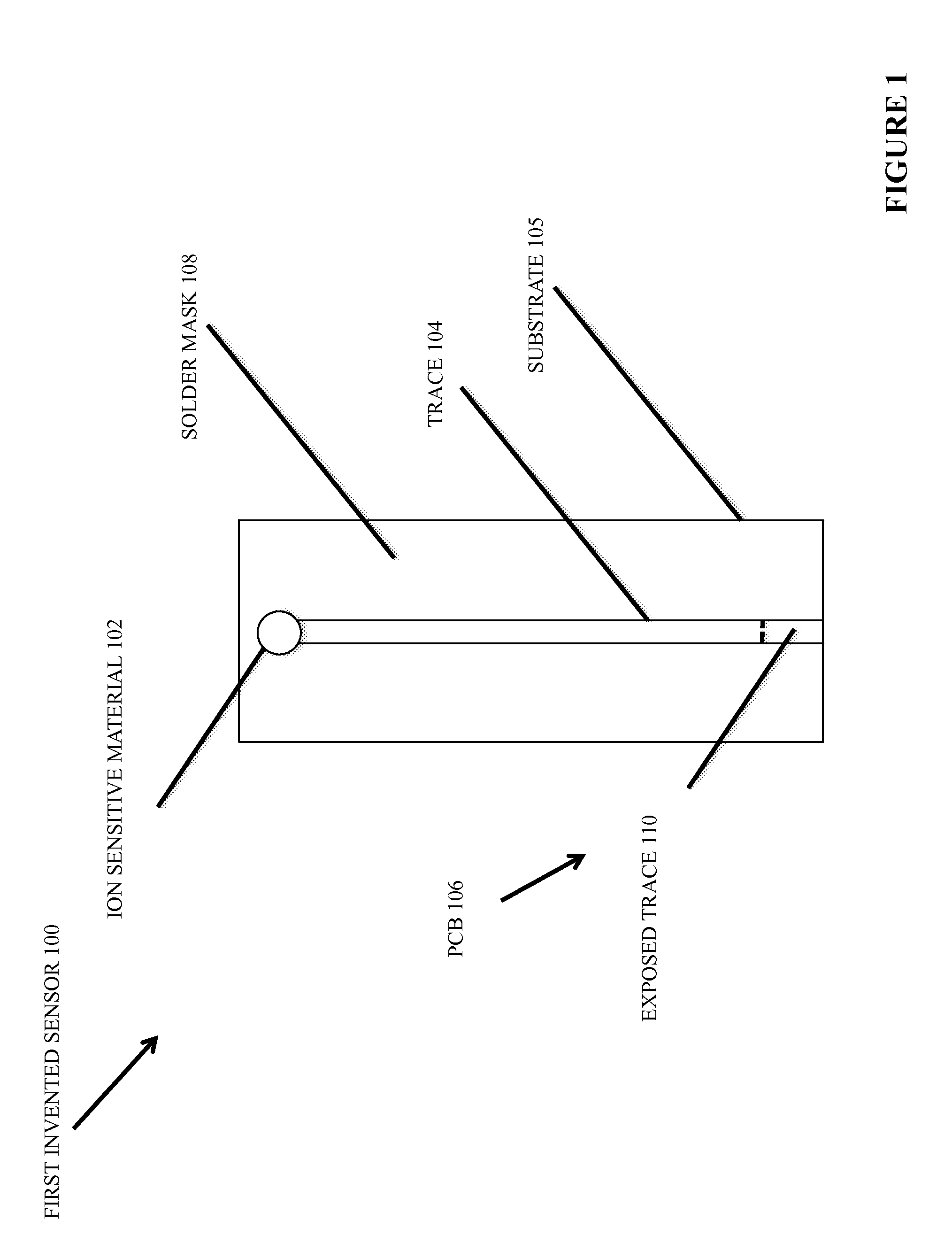
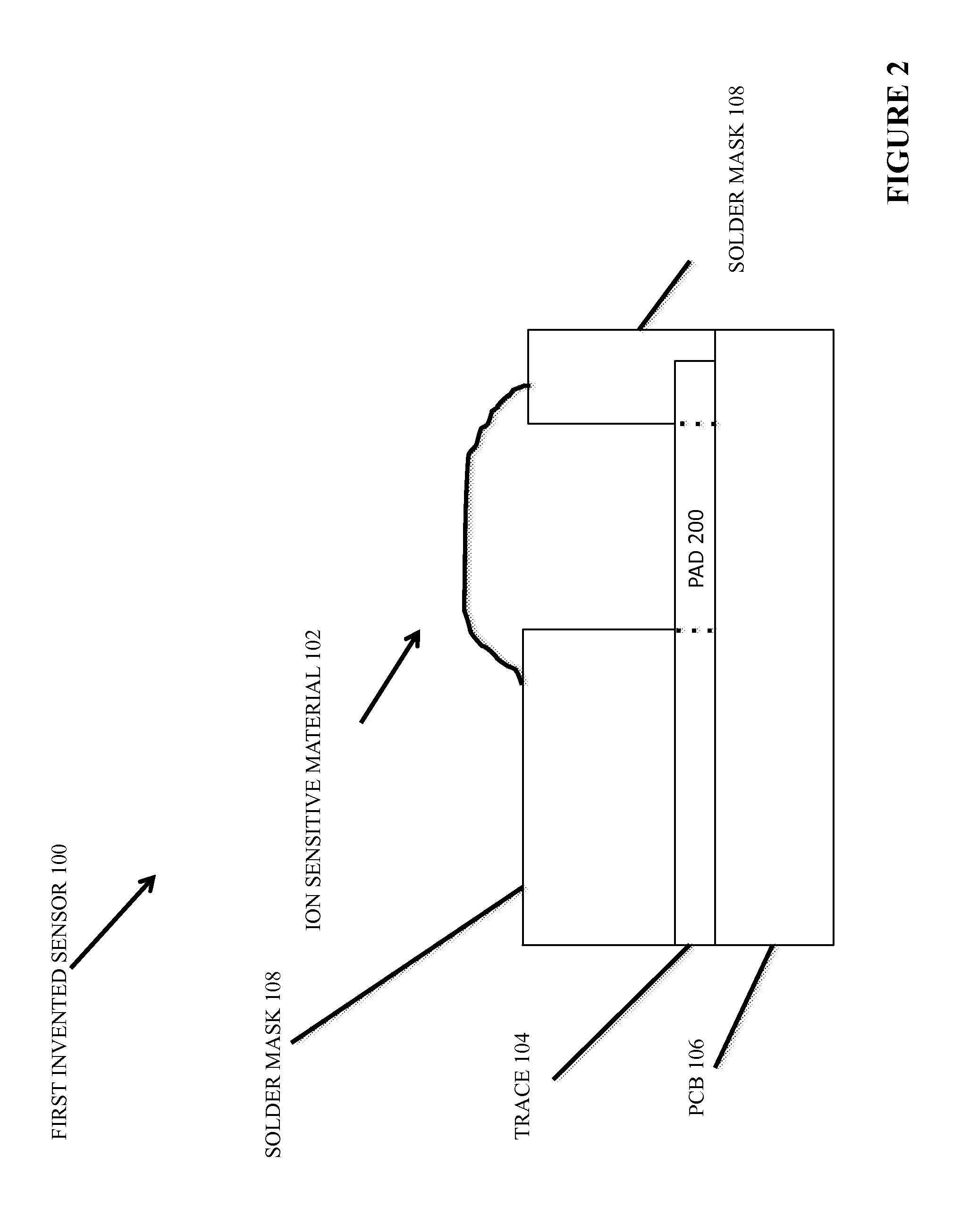
[0053]Referring generally to the Figures and particularly to FIG. 1, FIG. 1 is a top view of an invented sensor 100 that includes an ion sensitive material 102 electrically coupled with an electrically conductive trace 104 of a printed circuit board 106 (hereinafter “PCB”106). The trace 104 may comprise copper and is affixed to an insulating nonconductive substrate 105 of the PCB 106. The trace 104 extends from the ion sensitive material 102. A solder mask 108 in combination with the insulating nonconductive substrate 105 substantively shields the trace 104 from physical damage. An exposed trace le...
PUM
 Abstract
Description
Claims
Application Information
 - R&D Engineer
- R&D Manager
- IP Professional
- Industry Leading Data Capabilities
- Powerful AI technology
- Patent DNA Extraction
Browse by: Latest US Patents, China's latest patents, Technical Efficacy Thesaurus, Application Domain, Technology Topic.
© 2024 PatSnap. All rights reserved.Legal|Privacy policy|Modern Slavery Act Transparency Statement|Sitemap