Liquid crystal display, array substrate in in-plane switching mode and manufacturing method thereof

Active Publication Date: 2015-02-05
SHANGHAI AVIC OPTOELECTRONICS +1
View PDF4 Cites 1 Cited by
  • Summary
  • Abstract
  • Description
  • Claims
  • Application Information

AI Technical Summary

Benefits of technology

[0013]Since the pixel electrode is disposed in the groove of the first organic film and the common electrode is disposed on the surface of the first organic film outside the groove, the pixel electrode and the common electrode can be arranged on different planes of the same array substrate and can also be fo

Problems solved by technology

To sum up, currently there is no array substrate capable of simultaneously achieving a high transmittance and overcoming the

Method used


Image

  • Liquid crystal display, array substrate in in-plane switching mode and manufacturing method thereof
  • Liquid crystal display, array substrate in in-plane switching mode and manufacturing method thereof
  • Liquid crystal display, array substrate in in-plane switching mode and manufacturing method thereof

Examples


Example

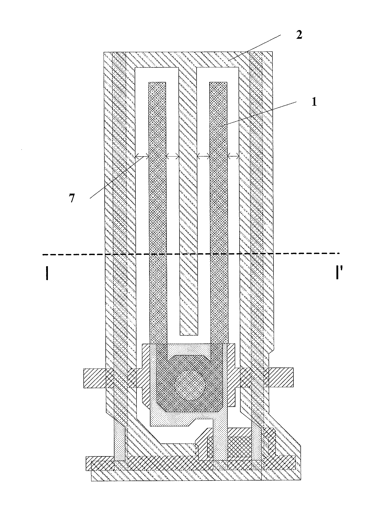
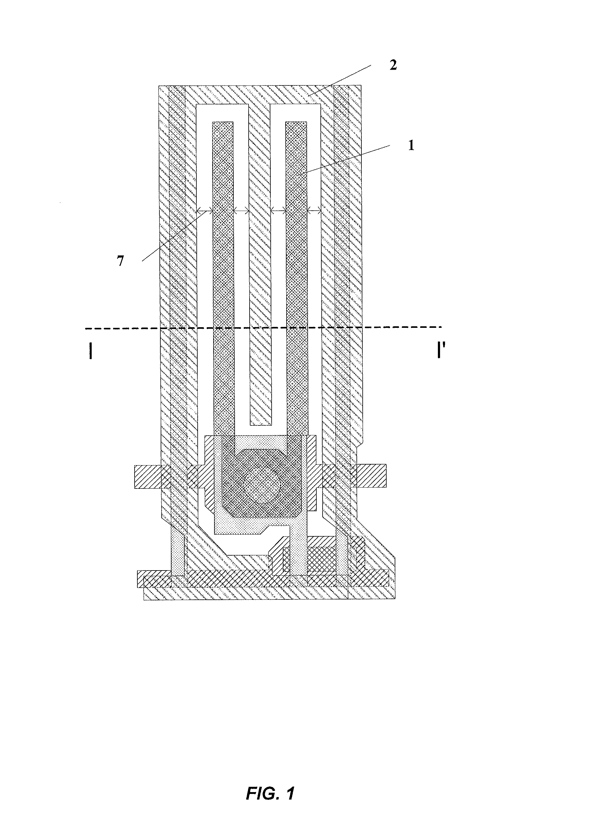
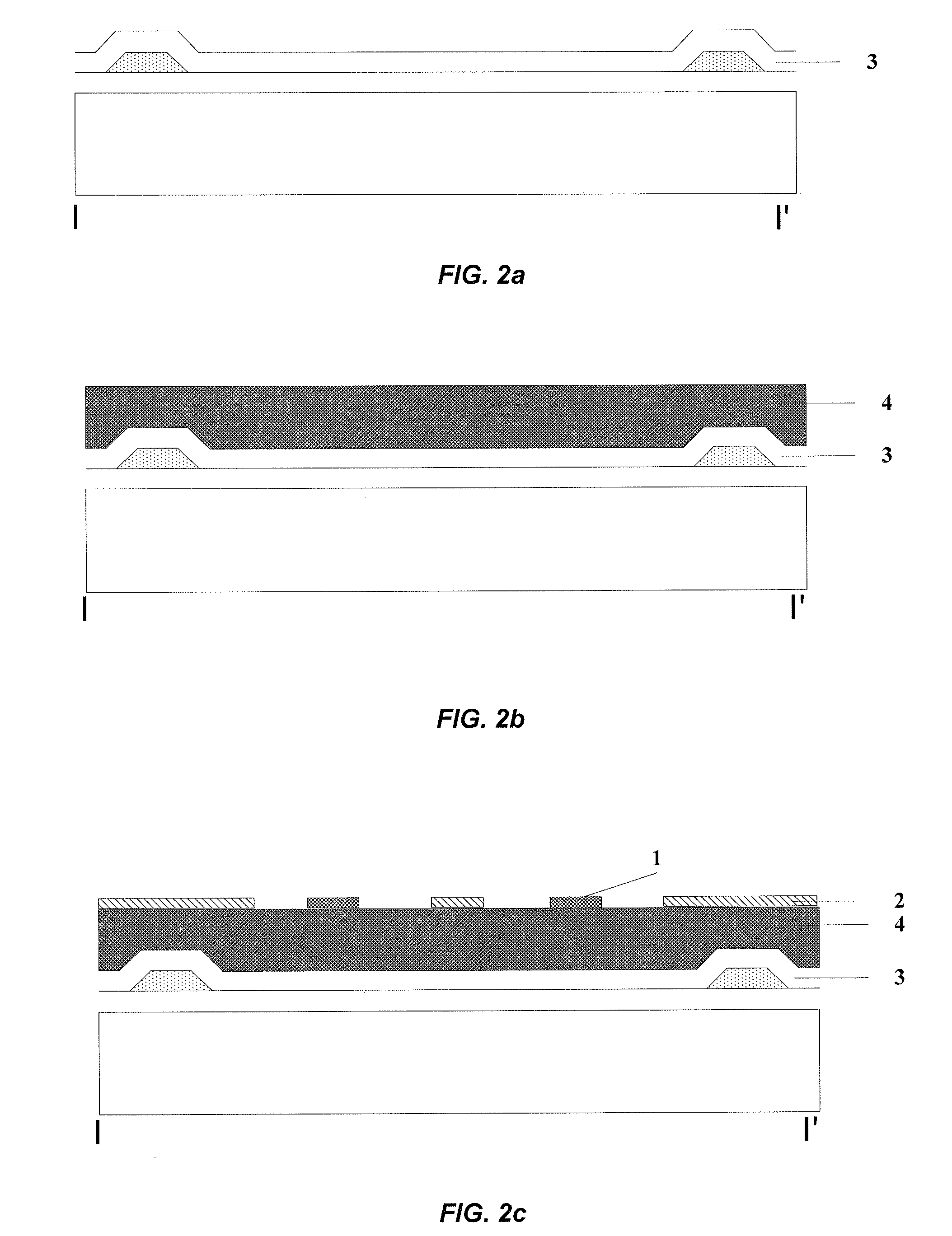
[0023]In order to solve the problem in the prior art that the array substrate in the IPS mode cannot simultaneously achieve the high transmittance and increase the precision of overlapping of the pixel electrode and the common electrode with respective preset positions, the inventor provides, through research, a liquid crystal display, an array substrate in an in-plane switching mode and a manufacturing method thereof. In the technical solution, since the pixel electrode is disposed in the groove of the first organic film and the common electrode is disposed on the surface of the first organic film outside the groove, the pixel electrode and the common electrode can be arranged on different planes of the same array substrate and can also be formed at one time, to thereby both ensure the light transmittance of the array substrate and accurately control the specific gaps between the pixel electrode and the common electrode, thus increasing the precision of overlapping of the pixel ele...


PUM


Abstract

An array substrate comprises a substrate, a passivation layer on a surface of the substrate, a first organic film on a surface of the passivation layer and provided with a groove, a common electrode disposed on a surface of the first organic film outside the groove, and a pixel electrode disposed in the groove. A vertical projection of the common electrode on the surface of the passivation layer does not overlap with a vertical projection of the pixel electrode on the surface of the passivation layer.

Description

CROSS-REFERENCES TO RELATED APPLICATIONS[0001]This application claims the benefit of priority to Chinese Patent Application No. 201310326466.6, filed with the Chinese Patent Office on Jul. 30, 2013 and entitled “LIQUID CRYSTAL DISPLAY, ARRAY SUBSTRATE IN IN-PLANE SWITCHING MODE AND MANUFACTURING METHOD THEREOF”, the content of which is incorporated herein by reference in its entirety.FIELD OF THE INVENTION[0002]The present invention relates to the field of display technologies, and in particular to a liquid crystal display, an array substrate in an in-plane switching mode and a manufacturing method thereof.BACKGROUND OF THE INVENTION[0003]Thin film transistor liquid crystal displays are developing more and more rapidly and have become mainstream flat panel displays. From the time they came out up to the present, multiple categories of thin film transistor liquid crystal displays have been developed, driving modes and display effects thereof are different, and each category has its o...

Claims


Application Information

Patent Timeline
IPC IPC(8): G02F1/1343
CPCG02F1/13439G02F1/134363G02F1/133345G02F1/134318G02F1/134372G02F1/134381
Inventor LIANG, YANFENG
Owner SHANGHAI AVIC OPTOELECTRONICS
Why Eureka
Try Eureka