Circuit Probe for Charged Particle Beam System

a technology of charged particle and circuit probe, which is applied in the field of electric probes, can solve the problems of inability to reduce the energy of electron beam, loss of much of the flexibility of dual beam,

Active Publication Date: 2015-02-19
FEI CO
View PDF3 Cites 3 Cited by
  • Summary
  • Abstract
  • Description
  • Claims
  • Application Information

AI Technical Summary

Benefits of technology

[0007]An object of the invention is to provide the flexibilit

Problems solved by technology

When a probe assembly is mounted in the dual beam system, however, much of the flexibility of the dual beam is lost.
The electronics of the probe assembly may prevent the application of a retarding voltage to the stage or sample, so that the electron beam energy cannot be reduced after passing the focusing

Method used


Image

  • Circuit Probe for Charged Particle Beam System
  • Circuit Probe for Charged Particle Beam System
  • Circuit Probe for Charged Particle Beam System

Examples


Embodiment Construction

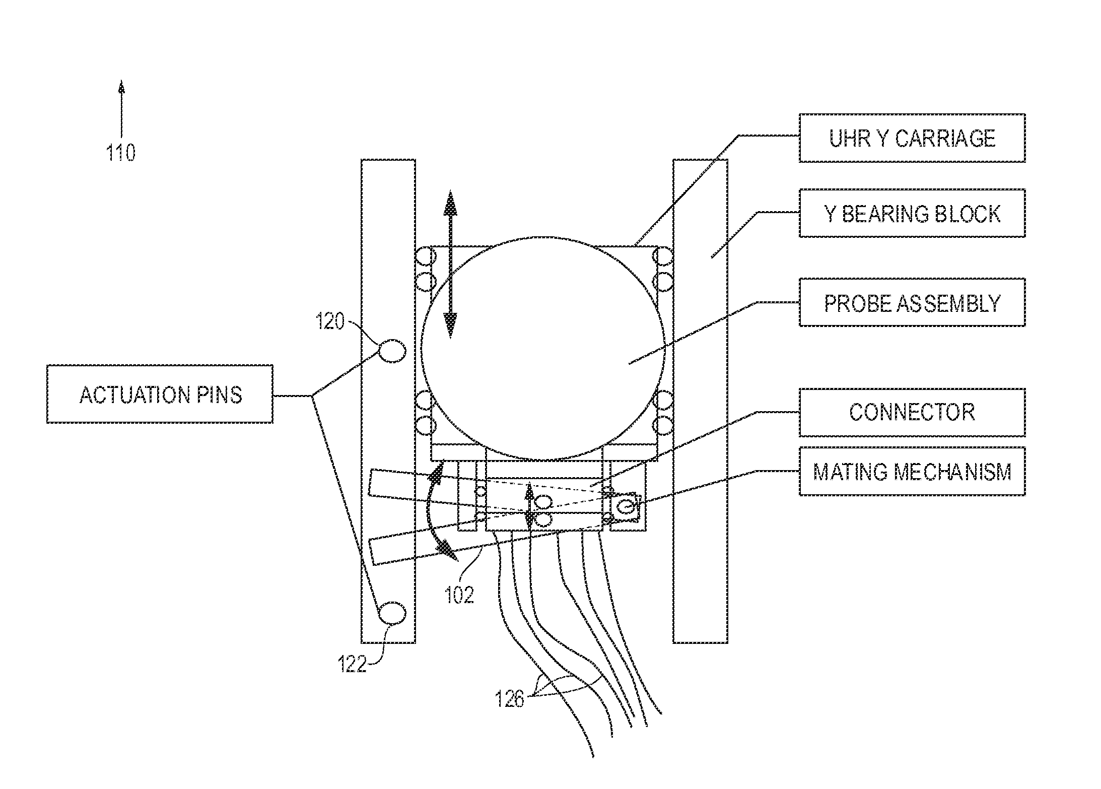
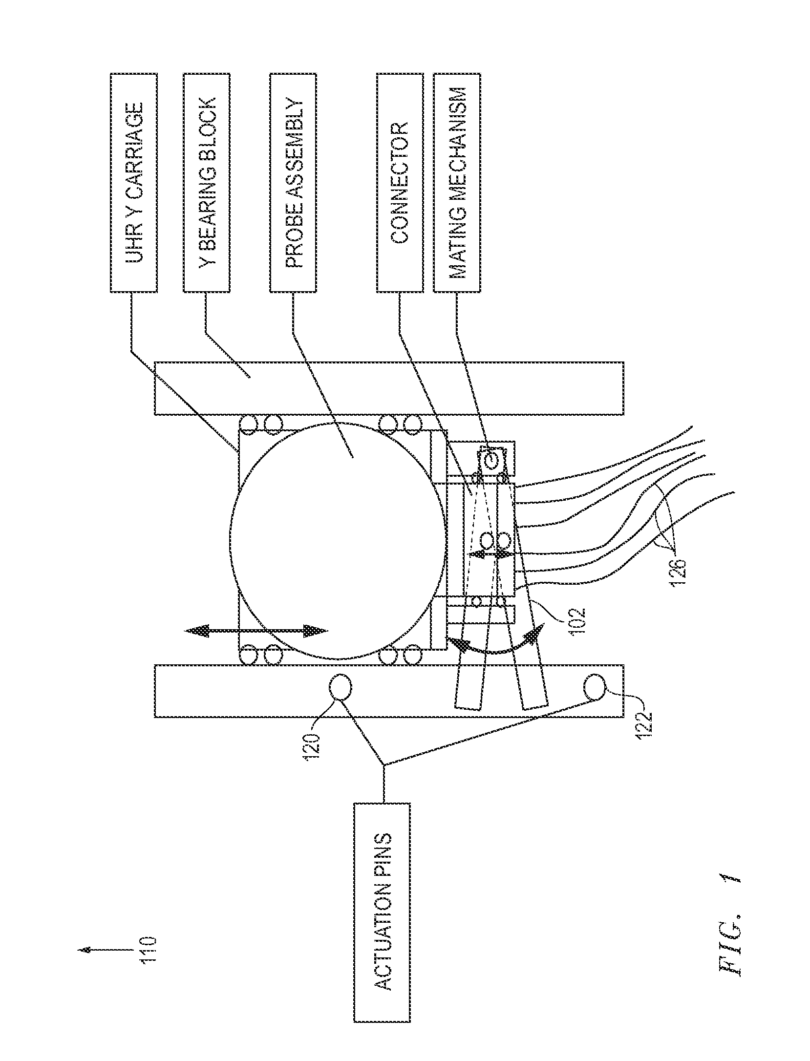
[0023]It is desirable to be able to switch back and forth between electrically testing a sample using a nanoprobe and processing the sample using charged particle beam processing without removing the sample from the vacuum chamber.

[0024]During processing, applicants have recognized that, in some sample preparation processes, it is desirable that:[0025]a. The sample region of interest is at the coincident point of the beams;[0026]b. The sample is grounded;[0027]c. The needles are grounded;[0028]d. The sample can tilt to 52 degrees; and[0029]e. While at 42 degrees tilt, the stage can rotate fully through + / −180 degrees.

[0030]The wiring harness that carries electrical signals to and from the probe assembly must be disconnected before tilting or rotating, and disconnecting will eliminate the ground connection from the sample and the needles. Also, the wiring harness must be disconnected before biasing the stage to a high voltage, which reducing the beam energy, to avoid damaging the pro...


PUM


Abstract

A probe assembly can be connected and disconnected from its electrical harness within a vacuum chamber so that the probe assembly with the work piece mounted can be rotated and tilted without interference from a cable, and can then be reconnected without opening the vacuum chamber. Also described is a means of grounding a sample and probes when the probe assembly is disconnected from its electrical harness and a means of preventing damage to the probe mechanism and the probe itself by ensuring that the probes are not sticking up too far during operations.

Description

CROSS-REFERENCE TO RELATED APPLICATIONS[0001]This application claims priority from U.S. Provisional Application 61 / 866,003 filed Aug. 14, 2013, which is hereby incorporated by reference.TECHNICAL FIELD OF THE INVENTION[0002]The present invention relates to electrical probes for use with charged particle beams systems.BACKGROUND OF THE INVENTION[0003]Using small conductors on the nanometer scale to probe electrical circuits is referred to as nanoprobing. Nanoprobing is widely used in the semiconductor market for failure analyses and device characterization. Some probes can be positioned with a resolution of better than 10 nm to measure or apply a voltage or current to electrically test a circuit.[0004]Before probing, the sample needs to be prepared, for example, by exposing buried conductors to electrically access a circuit. A dual beam system, that is, a charged particle beam system including an ion beam column and an electron beam column, is a powerful tool for sample analysis. In ...

Claims


Application Information

Patent Timeline
IPC IPC(8): G01R1/067
CPCG01R1/06705H01J9/02H01J49/08H01J37/20H01J2237/208H01J2237/24564H01J2237/24592H01J2237/2008H01J2237/206G01R1/06711
Inventor BARENDS, PAUL JOHANNES L.VAN DEN BOOGAARD, MATHIJS P.W.BRUNDAGE, PHILIP
Owner FEI CO
Why Eureka
Try Eureka