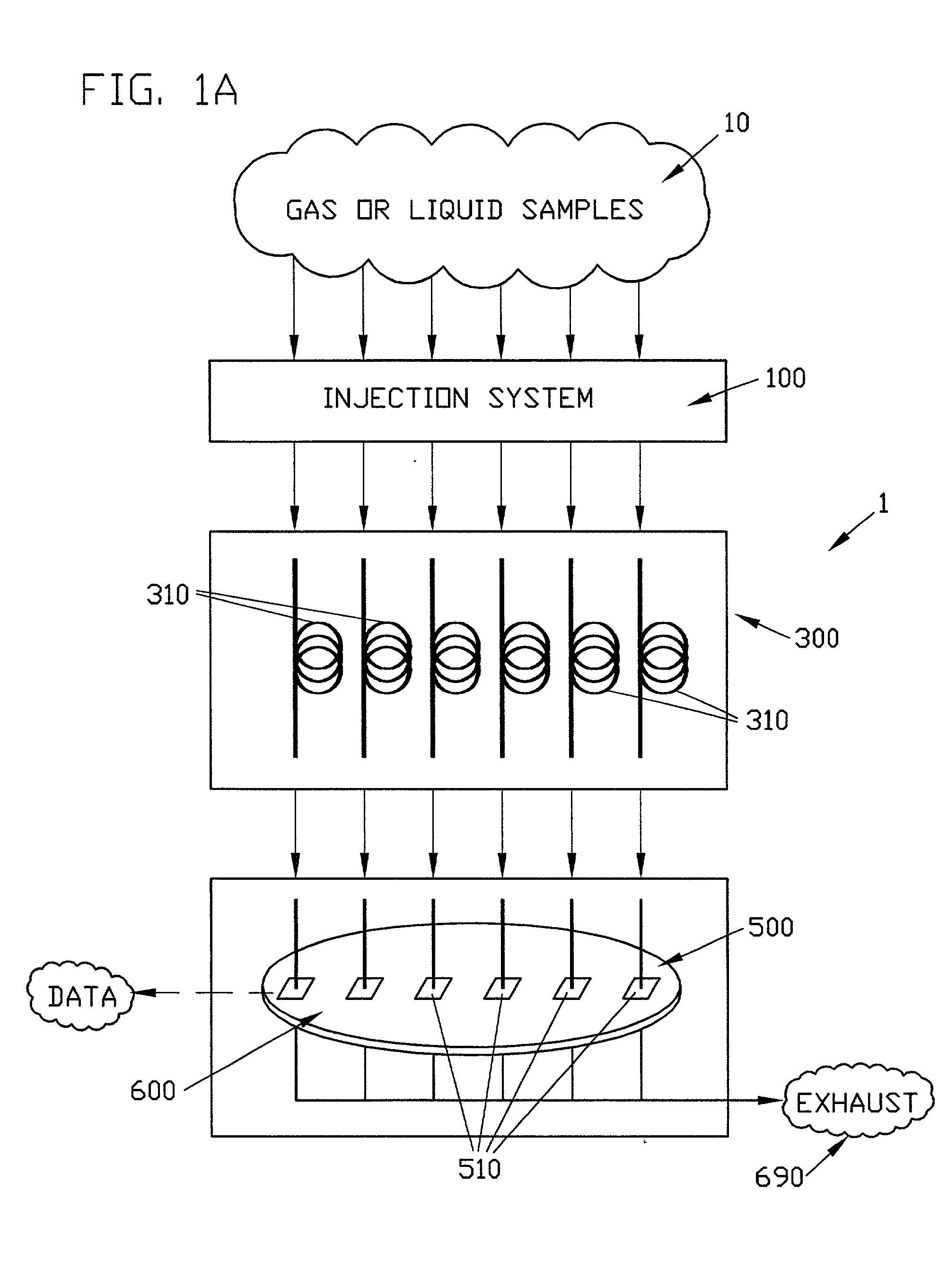
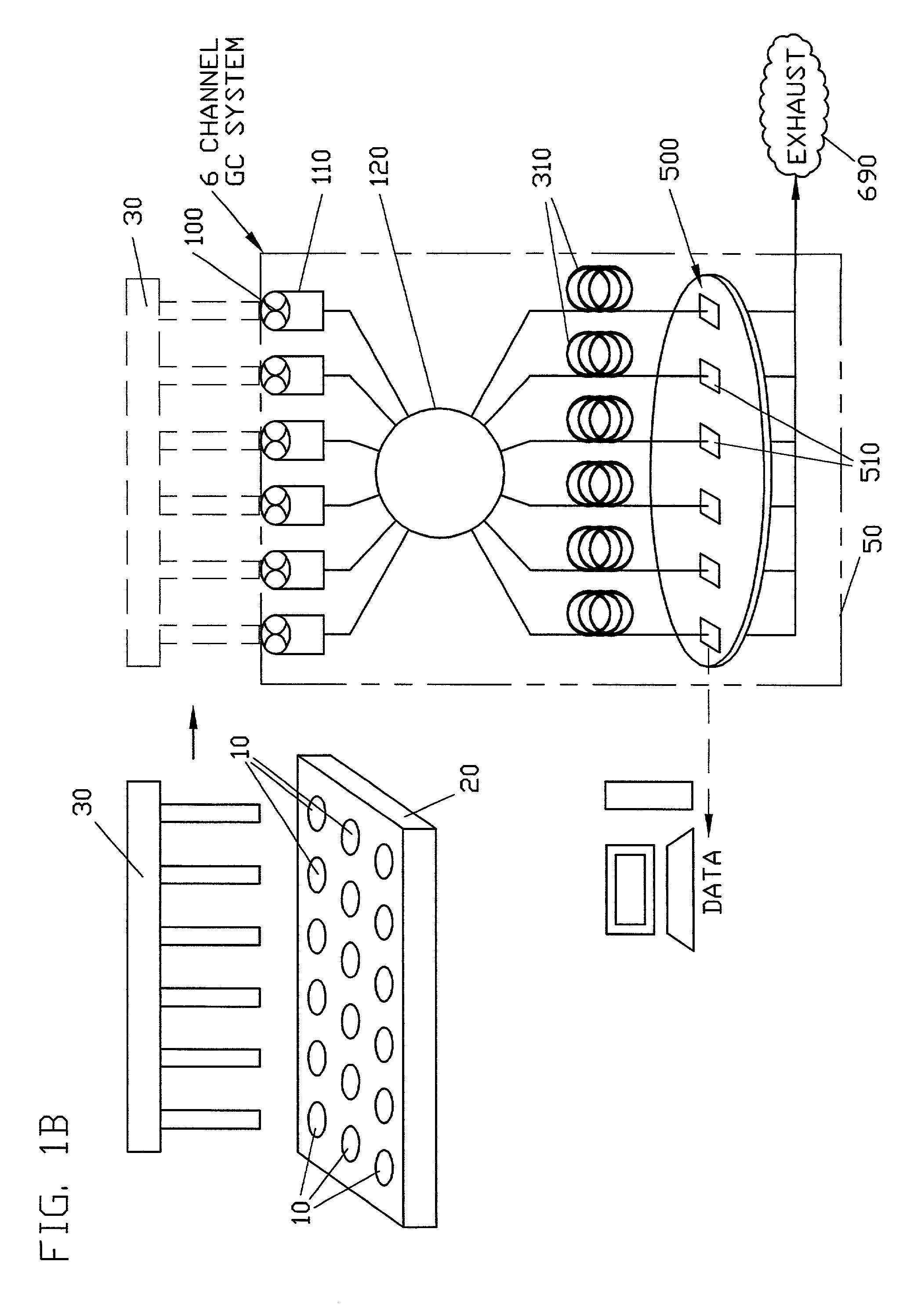
Parallel gas chromatograph with microdetector array
a gas chromatograph and microdetector technology, applied in the field of gas chromatography, can solve the problems of limited interchangeability of components, current state of the art suffers, and relatively bulky packaging
- Summary
- Abstract
- Description
- Claims
- Application Information
AI Technical Summary
Benefits of technology
Problems solved by technology
Method used
Image
Examples
example 1
Microfabrication of Integral Thermal Conductivity Detector
[0101] An array comprising microfabricated thermal conductivity detectors was made using substantially known prior art microfabrication techniques. Briefly, with reference to FIGS. 6A through 6P (and where indicated, also to FIGS. 5L and 5M), fabrication was effected as follows:
[0102] 1. Wafer 1 (bottom capillary wafer 620 (FIG. 5L), 400 .mu.m thick), and Water 2 (central filament wafer 610 (FIGS. 5L and 5M) 400 .mu.m thick) were provided. Both Wafer 1 and Wafer 2 were single-crystal silicon wafers (Si-wafers): oriented; 125 mm diameter; 400 .mu.m thickness; and double-sided polished.
[0103] 2. Wafer 1 was oxidized on both sides (oven at 1100.degree. C., wet, about 3.3 .mu.m thick).
[0104] 3. Wafer 1: spinning of photo resist on front side / baking.
[0105] 4. Wafer 1: spinning of photo resist on back side / baking.
[0106] 5. Wafer 1: double-sided photolithography (1) on front side of wafer (fluidic holes for inlet port and outlet po...
example 2
Microfabrication of Integral Thermal Conductivity Detector
[0156] In an alternative embodiment, an array comprising microfabricated thermal conductivity detectors was made using substantially known prior art microfabrication techniques. Briefly, with reference to FIGS. 10A through 10E, (and where indicated, also to FIGS. 7F and 7G), fabrication was effected as follows:
[0157] 1. A wafer (filament wafer 680 (FIGS. 7F and 7G), 400 .mu.m thick) was provided. The wafer was single-crystal silicon: oriented; 125 mm diameter; 400 .mu.m thickness; and double-sided polished.
[0158] 2. A SiN layer was deposited on both sides (LPCVD, 1 .mu.m thickness) (See FIG. 10A).
[0159] 3. The top side of the filament wafer 680 was subseqently patterned, and the filament 520 and contact pads 523, 524 were formed as Cr / Pt layers, substantially as described in Example 1. (See FIG. 10B).
[0160] 4. Both sides of the SiN were then patterned (using photolithography and etching) in preparation for formation of the d...
example 3
Analysis of Liquid Samples
[0166] A six-channel gas chromatograph instrument comprising an array of microdetctors as disclosed herein was used to screen a 96-sample microtiter plate using a 1% decane in benzene mixture in every well of the plate. The results of the chromatogram for six channels of a single run are shown in FIG. 9. The nitrogen peak is the residual purge gas present in the injection block and does not interfere with the chromatogram. Conventional gas chromatograms (GC's) use helium as the purge gas, which cannot be distinguished from the carrier gas which is also helium. The nitrogen peak in the parallel GC offers the ability to monitor for mis-injections. The nitrogen peak is typically very large in case of a bad injection (not shown in FIG. 9). The variation in peak area from run to run (after calibration) is less than 10%. The total run-time for the 96 samples was .about.58 minutes total, which is less than a factor of six compared with what would have been require...
PUM
| Property | Measurement | Unit |
|---|---|---|
| volume | aaaaa | aaaaa |
| volume | aaaaa | aaaaa |
| temperature | aaaaa | aaaaa |
Abstract
Description
Claims
Application Information


