Check patentability & draft patents in minutes with Patsnap Eureka AI!

Semiconductor device having high mobility channel

a technology of mobility channel and semiconductor, which is applied in the direction of semiconductor devices, electrical devices, transistors, etc., can solve the problems of increasing substrate leakage, and achieve the effects of reducing leakage, facilitating conductivity, and high mobility channel

Active Publication Date: 2015-04-02
QUALCOMM INC
View PDF1 Cites 22 Cited by
  • Summary
  • Abstract
  • Description
  • Claims
  • Application Information

AI Technical Summary

Benefits of technology

[0013]One particular advantage provided by at least one of the disclosed embodiments is that a semiconductor device having a high mobility channel is formed. The semiconductor device may advantageously include a high mobility channel that enables conductivity (e.g., high current) when the semiconductor device is in an on state. For example, a junction between the doped region and the source/drain region may enable a high-mobility

Problems solved by technology

However, the use of high mobility materials in the channel region of a semiconductor device may create certain prob

Method used


Image

  • Semiconductor device having high mobility channel
  • Semiconductor device having high mobility channel
  • Semiconductor device having high mobility channel

Examples


Embodiment Construction

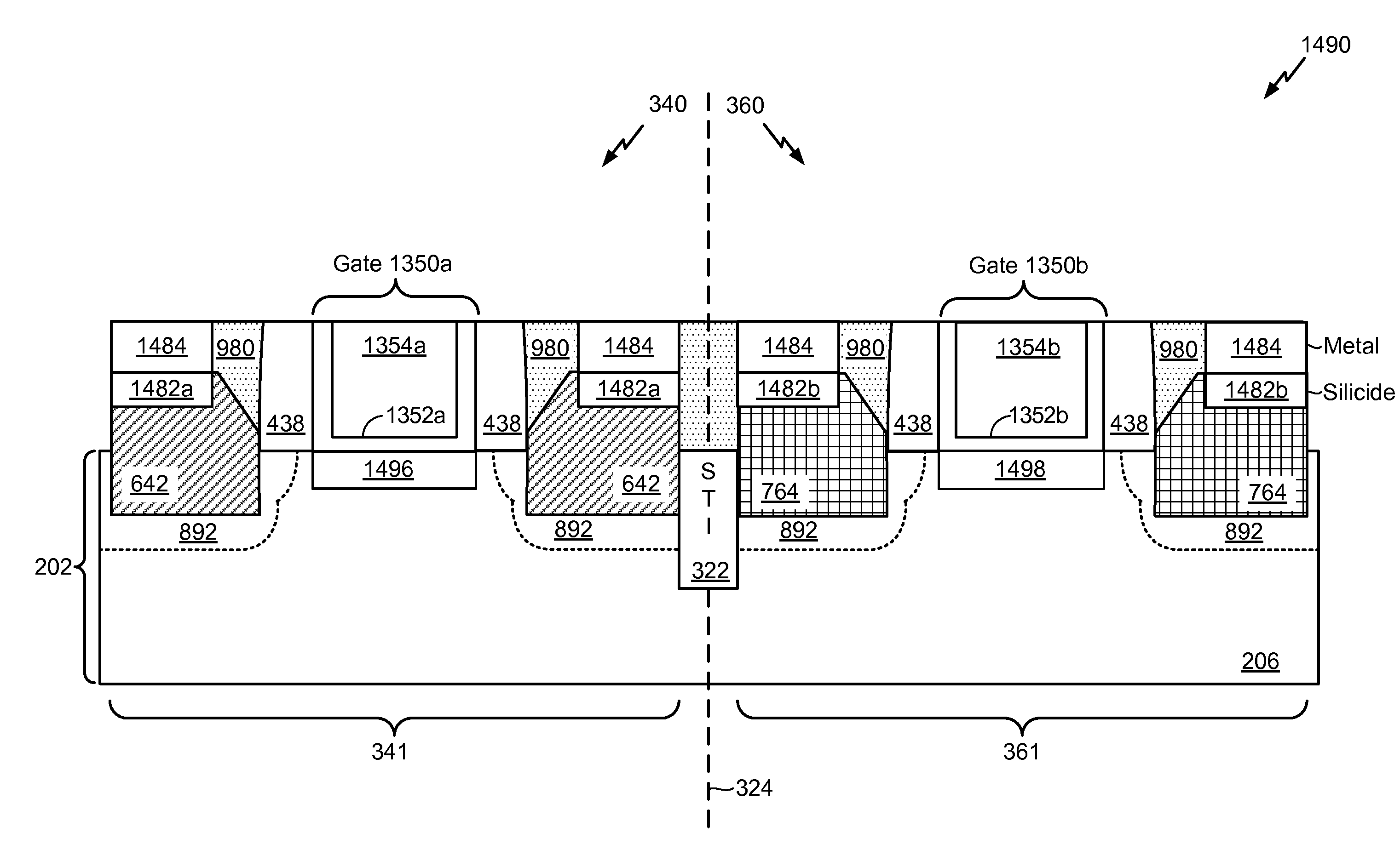
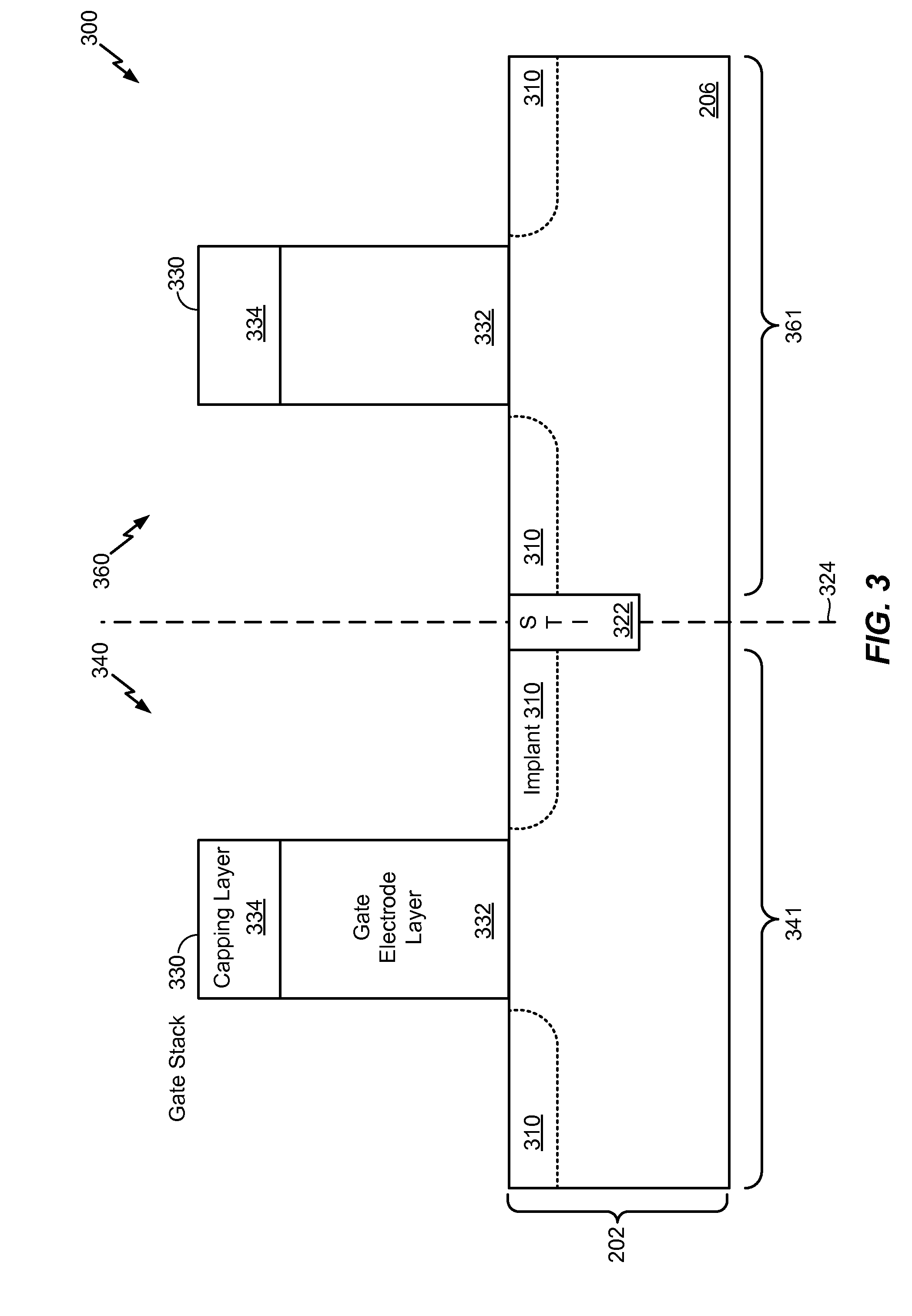
[0035]Particular embodiments of the present disclosure are described below with reference to the drawings. In the description, common features are designated by common reference numbers throughout the drawings.

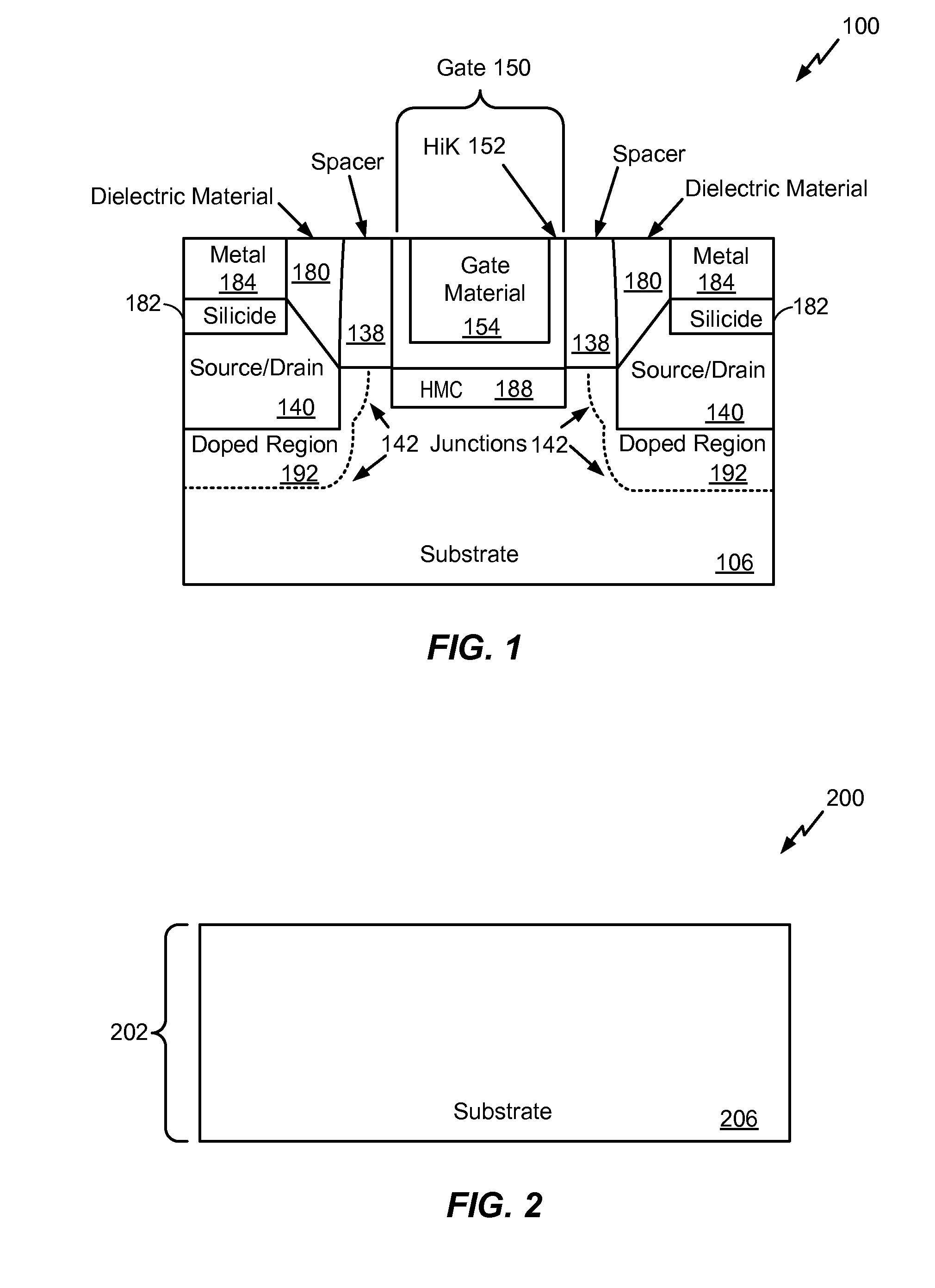
[0036]Referring to FIG. 1, a diagram of a semiconductor device 100 including a high mobility channel is shown. The semiconductor device 100 may include a complementary metal-oxide-semiconductor (CMOS) device, such as a p-type metal-oxide-semiconductor (pMOS) device or an n-type metal-oxide-semiconductor (nMOS) device.

[0037]The semiconductor device 100 includes a substrate 106, such as a silicon (Si) substrate. The substrate 106 may include source / drain (S / D) regions 140 and a high mobility channel (HMC) 188. The source / drain regions 140 (e.g., source / drain implants) may include silicon germanium (SiGe), embedded silicon (e-Si), embedded silicon carbon (e-Si:C), or silicon doped with phosphorous (Si:P). Each of the source / drain regions 140 may be associated with a corresponding...


PUM


Abstract

In a particular embodiment, a semiconductor device includes a high mobility channel between a source region and a drain region. The high mobility channel extends substantially a length of a gate. The semiconductor device also includes a doped region extending from the source region or the drain region toward the high mobility channel. A portion of a substrate is positioned between the doped region and the high mobility channel

Description

I. FIELD[0001]The present disclosure is generally related to a semiconductor device having a high mobility channel and formation thereof.II. DESCRIPTION OF RELATED ART[0002]Advances in technology have resulted in smaller apparatuses and more powerful computing devices. For example, there currently exist a variety of portable personal computing devices, including wireless computing devices, such as portable wireless telephones, personal digital assistants (PDAs), and paging devices that are small, lightweight, and easily carried by users. More specifically, portable wireless telephones, such as cellular telephones and internet protocol (IP) telephones, can communicate voice and data packets over wireless networks. Further, many such wireless telephones include other types of devices that are incorporated therein. For example, a wireless telephone can also include a digital still camera, a digital video camera, a digital recorder, and an audio file player. Also, such wireless telephon...

Claims


Application Information

Patent Timeline
IPC IPC(8): H01L29/66H01L29/778
CPCH01L29/778H01L29/66431H01L21/823807H01L29/66545H01L29/66651H01L21/823814H01L29/4966H01L29/517H01L29/6659H01L29/66621H01L29/66636H01L29/7834H01L29/1054H01L29/165
Inventor YANG, BINCHIDAMBARAM, PRZHU, JOHN JIANHONGCHOI, JIHONGYANG, DATODI, RAVI MAHENDRANALLAPATI, GIRIDHARGAN, CHOCK HINGCAI, MINGSENGUPTA, SAMIT
Owner QUALCOMM INC
Features
  • R&D
  • Intellectual Property
  • Life Sciences
  • Materials
  • Tech Scout
  • Unparalleled Data Quality
  • Higher Quality Content
  • 60% Fewer Hallucinations
Learn More