Compact electronics test system having user programmable device interfaces and on-board functions adapted for use with multiple devices under test and in various environments including ones in proximity to a radiation field

Active Publication Date: 2015-05-28
THE UNITED STATES OF AMERICA AS REPRESENTED BY THE SECRETARY OF THE NAVY
View PDF3 Cites 6 Cited by
  • Summary
  • Abstract
  • Description
  • Claims
  • Application Information

AI Technical Summary

Benefits of technology

[0009]One aspect of an embodiment of the invention permits testing of digital electronics in harsh environments. An exemplary system can fit within a forty eight-pin DIP footprint that is capable of performing tests on digital electronic systems while being small enough to be highly portable and capable of being shielded properly when exposed to high levels of radiation in harsh environments (e.g., space). Exemplary aspects of an embodiment of the invention can be small enough to fit within a structure of a DUT board. Some embodiments can include a structure adapted to position a DUT over an aperture in supporting structure, such as a DUT board or another structure, which permits radiation in a test or operational environment to pass through the aperture with radiation sensitive supporting structures or components positioned around the aperture. The aperture also permits radiation source vectors to be applied to either side of a DUT and minimize direct exposure of radiation sources that otherwise pass directly through a DUT or component placed in a position of a DUT.
[0010]One aspect of the inve

Problems solved by technology

Current systems used to test digital components are large and expensive to create.
Existing testers are often extremely heavy, bulky, and not easily portable.
Existing systems also are not suitable for use in various testing environments such as radiation testing or operational configurations where radiation is present.
Existing test

Method used


Image

  • Compact electronics test system having user programmable device interfaces and on-board functions adapted for use with multiple devices under test and in various environments including ones in proximity to a radiation field
  • Compact electronics test system having user programmable device interfaces and on-board functions adapted for use with multiple devices under test and in various environments including ones in proximity to a radiation field
  • Compact electronics test system having user programmable device interfaces and on-board functions adapted for use with multiple devices under test and in various environments including ones in proximity to a radiation field

Examples


Example

DETAILED DESCRIPTION OF THE DRAWINGS

[0028]The embodiments of the invention described herein are not intended to be exhaustive or to limit the invention to precise forms disclosed. Rather, the embodiments selected for description have been chosen to enable one skilled in the art to practice the invention.

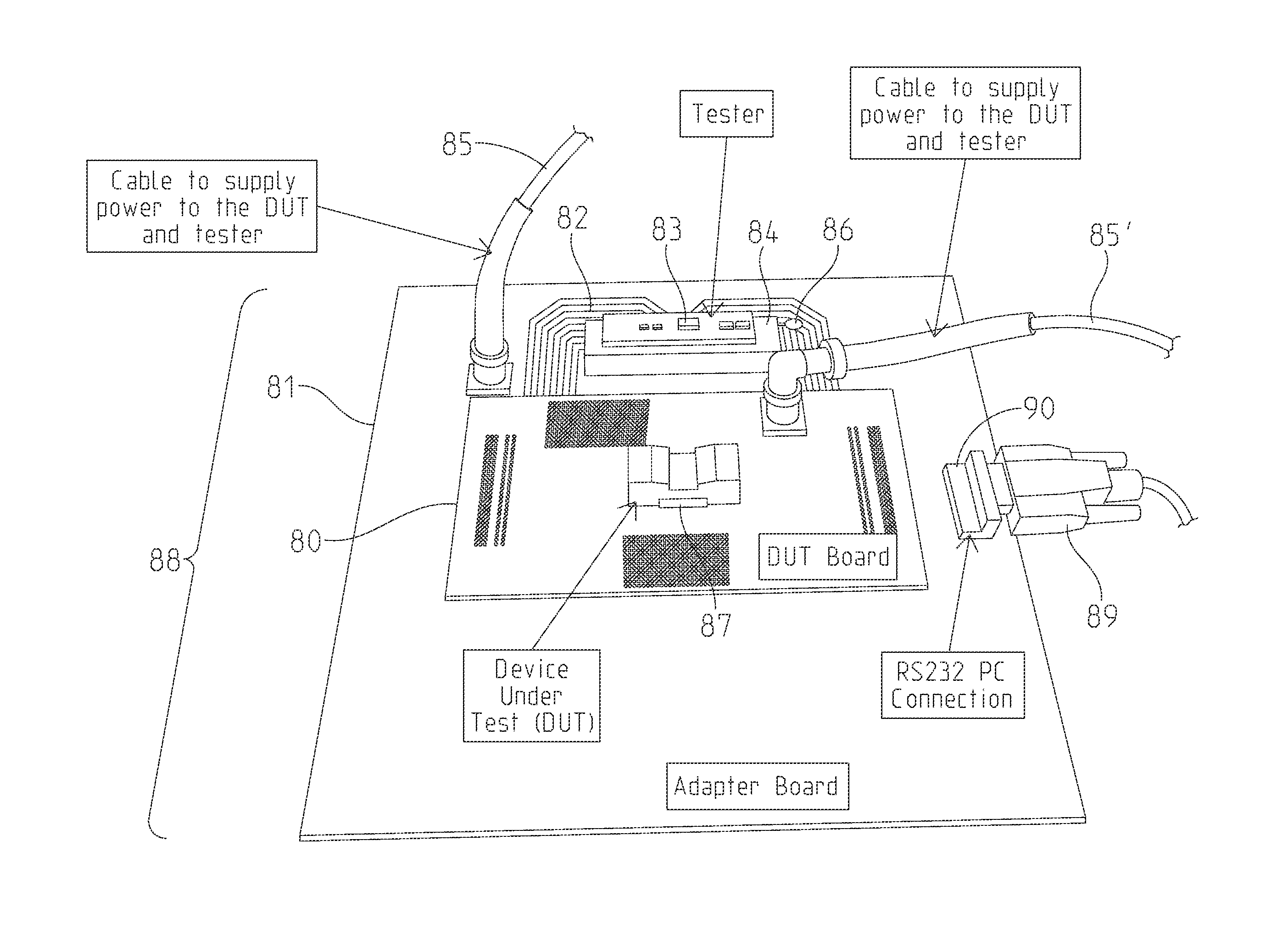
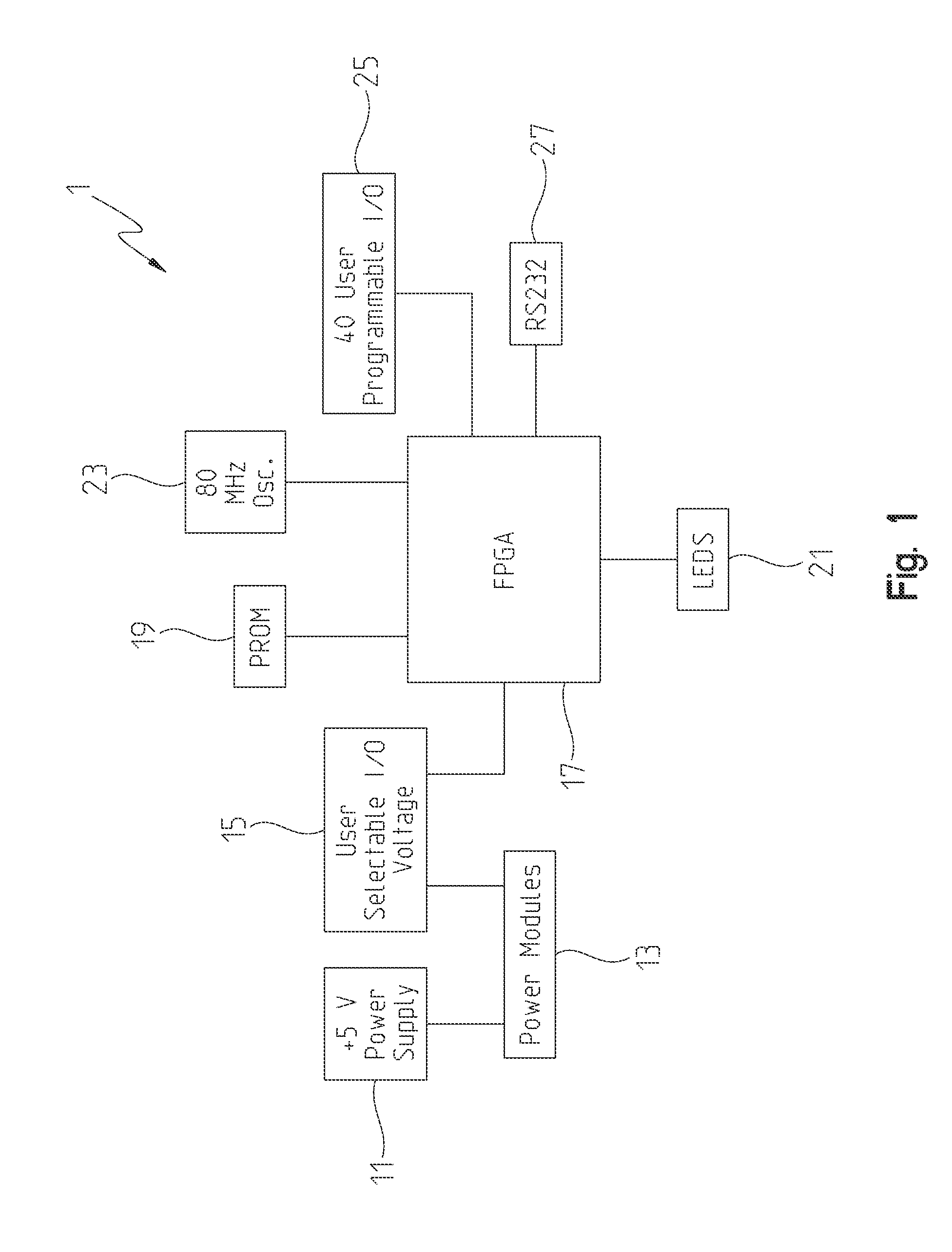
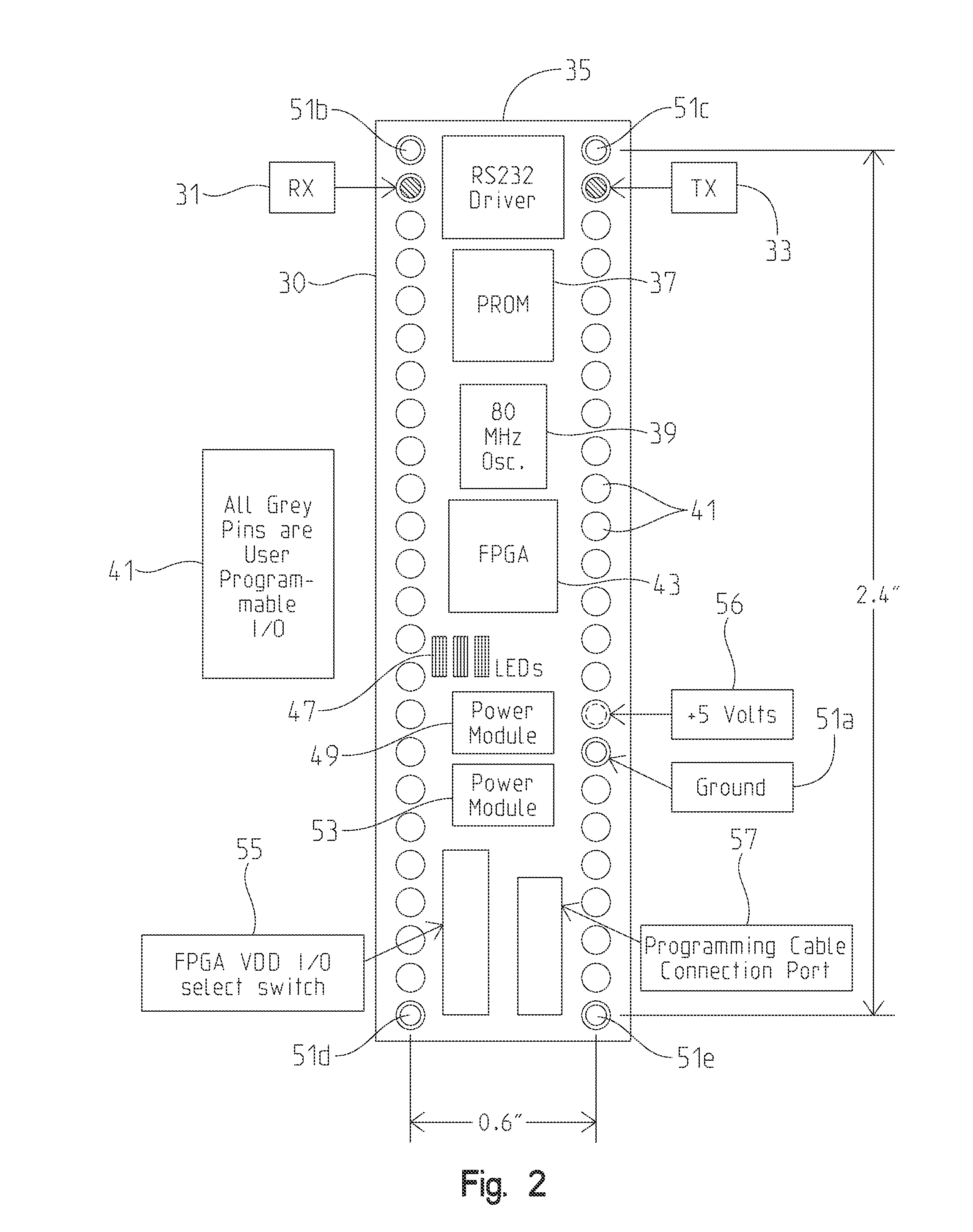
[0029]In general, according to an illustrative embodiment of the invention, one variant of an exemplary test system can include a FPGA based system that is placed on a tester structure, e.g., a printed circuit board with a footprint of 0.6 in×2.4 in dimensions that works with one or more test system interface structures. One embodiment can be designed to ensure that an entire exemplary test capability accommodates a standard forty-eight-pin DIP footprint which programmably interfaces to a DUT in a variety of ways. An embodiment of the invention can have forty programmable I / O structures which can be set to operate at, e.g., 1.2V, 1.5V, 1.8V, 2.5V, and 3.3V via a user selectable FPGA ...


PUM

PropertyMeasurementUnit
Electric potential / voltageaaaaaaaaaa

Abstract

Various apparatus and methods associated with a compact electronics test system having user programmable device interfaces and on-board functions adapted for use in various environments are provided. Exemplary embodiments can include a variety of apparatuses and methods to realize an advanced field programmable gate array adapted to perform functional tests on digital electronics within an exemplary 48-pin DIP footprint. One aspect of the invention can include a testing device comprised of components to produce a product that is inexpensive and consumable. A small size of an exemplary embodiment of the invention further allows for desirable shielding to be placed around a highly portable and highly programmable and adaptable testing device in order to protect it from external dangers found in harsh environments (e.g., high levels of radiation when operating in space, etc).

Description

CROSS-REFERENCE TO RELATED APPLICATIONS[0001]The present application claims priority to U.S. Provisional Patent Application Ser. No. 61 / 907,739, filed Nov. 22, 2013, entitled “COMPACT ELECTRONICS TEST SYSTEM HAVING USER PROGRAMMABLE DEVICE INTERFACES AND ON-BOARD FUNCTIONS ADAPTED FOR USE IN PROXIMITY TO A RADIATION FIELD,” the disclosure of which is expressly incorporated by reference herein.STATEMENT REGARDING FEDERALLY SPONSORED RESEARCH OR DEVELOPMENT[0002]The invention described herein was made in the performance of official duties by employees of the Department of the Navy and may be manufactured, used and licensed by or for the United States Government for any governmental purpose without payment of any royalties thereon. This invention (Navy Case 103,034) is assigned to the United States Government and is available for licensing for commercial purposes. Licensing and technical inquiries may be directed to the Technology Transfer Office, Naval Surface Warfare Center Crane, em...

Claims


Application Information

Patent Timeline
IPC IPC(8): G01R31/319G01R3/00G01R31/317
CPCG01R31/31905G01R3/00G01R31/31728G01R31/31721G01R1/18G01R31/31914Y10T29/49002
Inventor DUNCAN, ADAMGADLAGE, MATTHEW
Owner THE UNITED STATES OF AMERICA AS REPRESENTED BY THE SECRETARY OF THE NAVY
Why Eureka
Try Eureka