Liquid crystal display device
- Summary
- Abstract
- Description
- Claims
- Application Information
AI Technical Summary
Benefits of technology
Problems solved by technology
Method used
Image

Examples
first embodiment
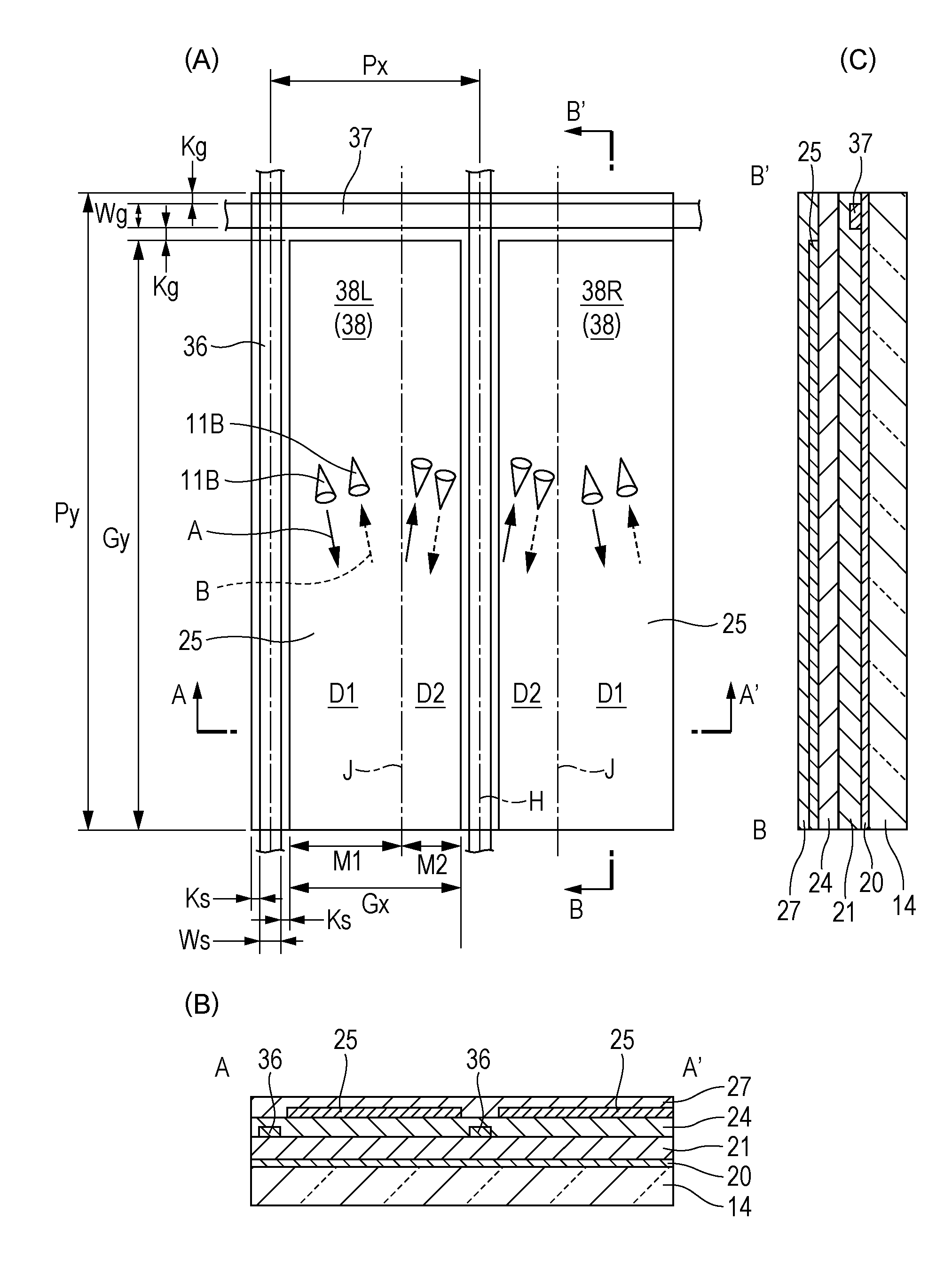
[0043]Hereinafter, a first embodiment of the present invention will be described with reference to FIGS. 1 to 12.
[0044]A liquid crystal display device according to the present embodiment is an example of a VA-mode liquid crystal display device in which two domains are provided in one sub pixel.
[0045]FIG. 1 is a cross-sectional view illustrating a liquid crystal display device according to the present embodiment.
[0046]It should be noted that, in the following drawings, in order to allow components to be seen easily, the components may be shown with dimensions at different scales.
[0047]The liquid crystal display device 1 according to the present embodiment includes, as shown in FIG. 1, a liquid crystal panel 13 and a backlight 8. The liquid crystal panel 13 includes a first polarization plate 3, a first phase difference plate 4, a liquid crystal cell 5, a second phase difference plate 6, and a second polarization plate 7. The backlight 8 is disposed below the liquid crystal panel 13 o...
second embodiment
[0121]Hereinafter, a second embodiment of the present invention will be described with reference to FIGS. 13 to 14.
[0122]A basic configuration of the liquid crystal display device according to the present embodiment is the same as that of the first embodiment except that the directions of the directors of the liquid crystal molecules are different from those of the first embodiment.
[0123]FIG. 13 is a plan view illustrating the two sub pixels adjacent to each other in the liquid crystal display device according to the present embodiment. FIG. 14 is a diagram illustrating simulation results of the alignment states of the liquid crystal molecules to which a voltage is applied, in the liquid crystal display device according to the present embodiment.
[0124]In FIGS. 13 and 14, the components, which are the same as those in the drawings for the first embodiment, are represented by the same reference numerals and signs, and the description thereof will be omitted.
[0125]In the case of the li...
third embodiment
[0130]Hereinafter, a third embodiment of the present invention will be described with reference to FIGS. 15 to 17.
[0131]A basic configuration of the liquid crystal display device according to the present embodiment is the same as that of the first embodiment except that the directions of the directors of the liquid crystal molecules are different from those of the first embodiment.
[0132]FIG. 15 is a plan view illustrating the two sub pixels adjacent to each other in the liquid crystal display device according to the present embodiment. FIG. 16 is a diagram illustrating simulation results of the alignment states of the liquid crystal molecules to which a voltage is applied, in the liquid crystal display device according to the present embodiment. FIG. 17 is a plan view illustrating the two sub pixels adjacent to each other in the liquid crystal display device according to a modification example of the present embodiment.
[0133]In FIGS. 15 to 17, the components, which are the same as t...
PUM
 Abstract
Description
Claims
Application Information
 - R&D Engineer
- R&D Manager
- IP Professional
- Industry Leading Data Capabilities
- Powerful AI technology
- Patent DNA Extraction
Browse by: Latest US Patents, China's latest patents, Technical Efficacy Thesaurus, Application Domain, Technology Topic.
© 2024 PatSnap. All rights reserved.Legal|Privacy policy|Modern Slavery Act Transparency Statement|Sitemap