
Display device and method for manufacturing the same

a technology of display device and display screen, which is applied in the field of flexible display device, can solve the problems of degrading the viewability of the display screen or being partially damaged, and achieve the effect of degrading the viewability of the display screen

Active Publication Date: 2015-09-10
JAPAN DISPLAY INC
View PDF3 Cites 52 Cited by
  • Summary
  • Abstract
  • Description
  • Claims
  • Application Information

AI Technical Summary

Benefits of technology

The present invention provides a well-controlled bend structure of a display panel and a method for manufacturing the display panel to solve the problem of degrading viewability of its screen or being partially damaged by stress concentration. The display panel substrate has a linear groove on at least part of a second principal surface of the flexible display panel substrate, and an electronic circuit substrate joined to a portion of the image display panel so that the portion does not intersect with the extension of the groove. The grooves are filled with an elastic material with a lower elastic modulus than a material of the flexible display panel substrate. The method for manufacturing the display device includes a resin being stacked on a support substrate having a linear ridge on at least part of the surface of the support substrate, the surface shape of the support substrate is transferred to the resin so that the groove is molded, the display panel substrate made of the resin is formed on the support substrate, the display elements are formed on the display panel substrate, and the support substrate is removed from the display panel substrate. This manufacturing method allows for the formation of a panel structure that can be integrally formed for multiple image display panels and can be cut into individual display panels.

Problems solved by technology

A display panel that can freely bend according to external forces may degrade the viewability of its screen or be partially damaged by stress concentration.

Method used


Image

  • Display device and method for manufacturing the same
  • Display device and method for manufacturing the same
  • Display device and method for manufacturing the same

Examples


Embodiment Construction

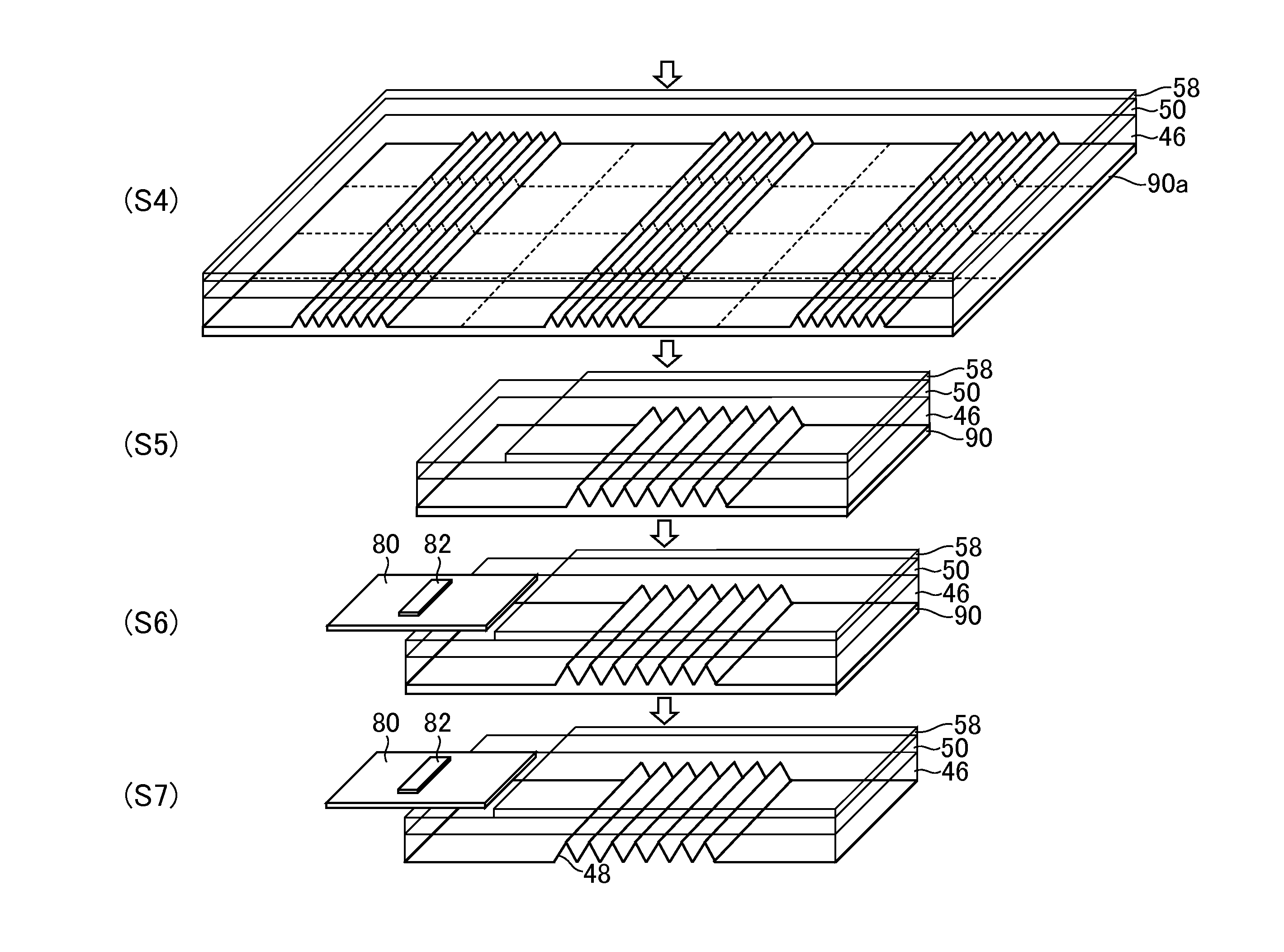
[0025]Embodiments of the present invention will now be described with reference to the accompanying drawings.

[0026]The disclosure herein is merely an example, and appropriate modifications coming within the spirit of the present invention, which are easily conceived by those skilled in the art, are intended to be included within the scope of the invention as a matter of course. The accompanying drawings schematically illustrate widths, thicknesses, shapes, or other characteristics of each part for clarity of illustration, compared to actual configurations. However, such a schematic illustration is merely an example and not intended to limit the present invention. In the present specification and drawings, some elements identical or similar to those shown previously are denoted by the same reference signs as the previously shown elements, and thus repetitive detailed descriptions of them may be omitted as appropriate.

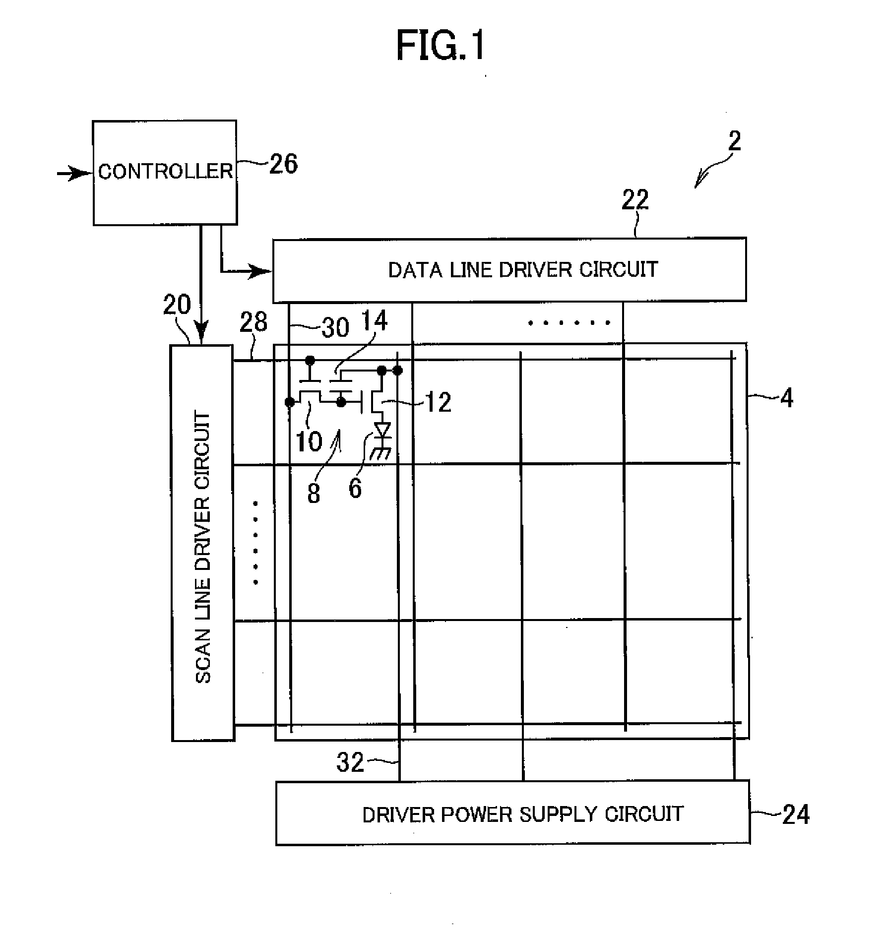
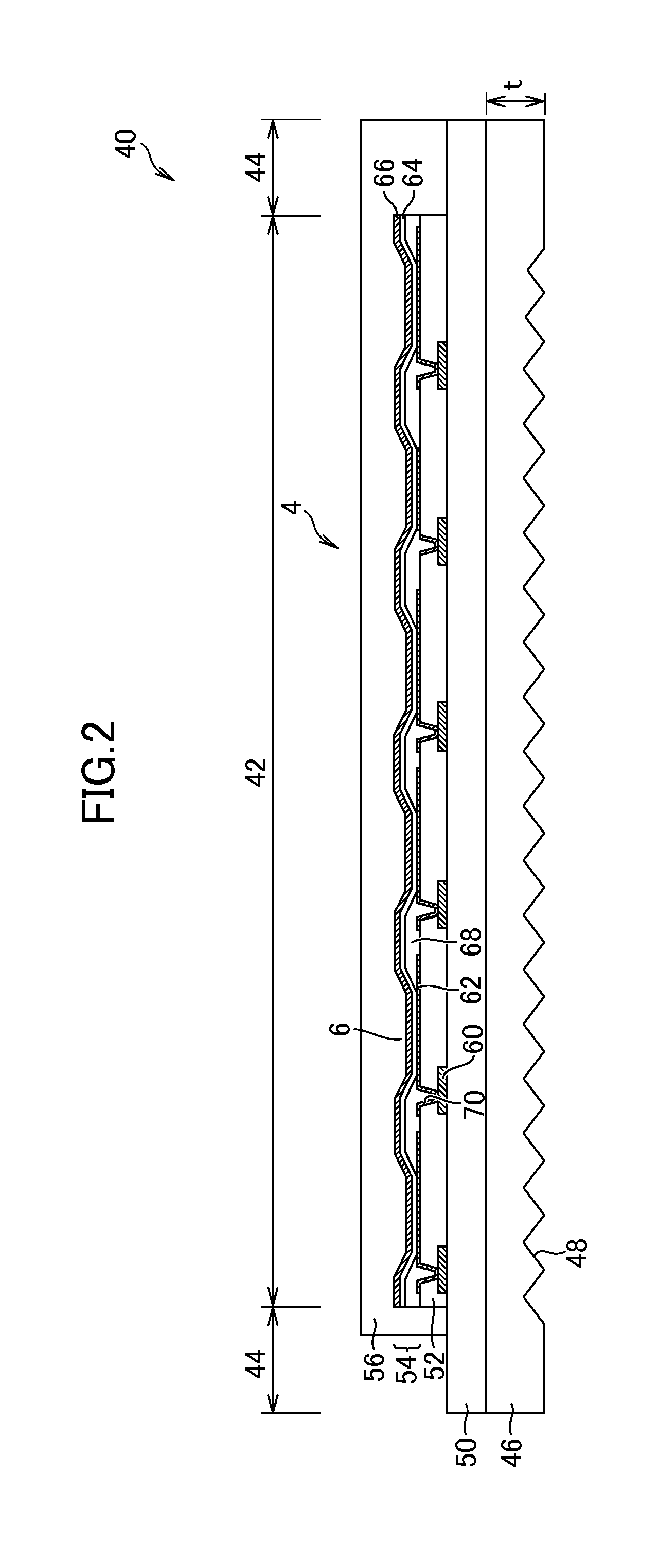
[0027]A display device according to an embodiment of the present in...


PUM


Abstract

How a flat panel display is bent by external forces is controlled. A display panel 40 has display elements, formed corresponding to the arrangement of pixels, on a first principal surface of a flexible display panel substrate 46. The display panel substrate 46 has a linear groove 48 on at least part of a second principal surface of the display panel substrate 46. A resin is stacked on a support substrate having a linear ridge on at least part of the surface of the support substrate. The surface shape of the support substrate is transferred to the resin so that the groove 48 is molded. Thus, the display panel substrate 46 made of the resin is formed on the support substrate. After the display elements are formed on the display panel substrate 46, the support substrate is removed from the display panel substrate 46.

Description

CROSS-REFERENCE TO RELATED APPLICATION[0001]The present application claims priority from Japanese application JP2014-042677 filed on Mar. 5, 2014, the content of which is hereby incorporated by reference into this application.BACKGROUND OF THE INVENTION[0002]1. Field of the Invention[0003]The present invention relates to a display device and a method for manufacturing the display device. In particular, the invention relates to a flexible display.[0004]2. Description of the Prior Art[0005]Flat panel displays, such as an organic electroluminescence (EL) display device, have a display panel including a thin film transistor (TFT) or an organic light-emitting diode (OLED) on a substrate. Glass substrates have been used as the substrate of such display panels. On the other hand, flexible displays, which have a flexible display panel with a substrate including a resin film, have been developed in recent years.SUMMARY OF THE INVENTION[0006]A display panel that can freely bend according to e...

Claims


Application Information

Patent Timeline
IPC IPC(8): H01L27/32H01L51/56H01L51/00
CPCH01L27/3244H01L51/0097H01L51/56H01L2251/5338H01L2227/323H01L2227/326H01L2251/566H01L51/003Y02E10/549Y02P70/50H10K71/80H10K77/111H10K59/1201H10K2102/311H10K59/12H10K50/844H10K71/00H10K71/851H10K2102/00H01L25/18
Inventor SATO, TOSHIHIROSASAKI, TOHRU
Owner JAPAN DISPLAY INC
Features
  • Generate Ideas
  • Intellectual Property
  • Life Sciences
  • Materials
  • Tech Scout
  • Unparalleled Data Quality
  • Higher Quality Content
  • 60% Fewer Hallucinations
Learn More