Method and system for a low parasitic silicon high-speed phase modulator

a phase modulator and low parasitic silicon technology, applied in the field of semiconductor processing, can solve the problems of cable bulk penalties, large power requirements, and complex structure, and achieve only modest improvements in reach and limited scalability

Active Publication Date: 2015-11-05
CISCO TECH INC
View PDF3 Cites 22 Cited by
  • Summary
  • Abstract
  • Description
  • Claims
  • Application Information

AI Technical Summary

Benefits of technology

[0005]A system and/or method for a low-parasitic silicon high-speed phase modulator, substantially as show...

Problems solved by technology

They can be mitigated to some extent with equalization, coding, and shielding, but these techniques require considerab...

Method used


Image

  • Method and system for a low parasitic silicon high-speed phase modulator
  • Method and system for a low parasitic silicon high-speed phase modulator
  • Method and system for a low parasitic silicon high-speed phase modulator

Examples


Embodiment Construction

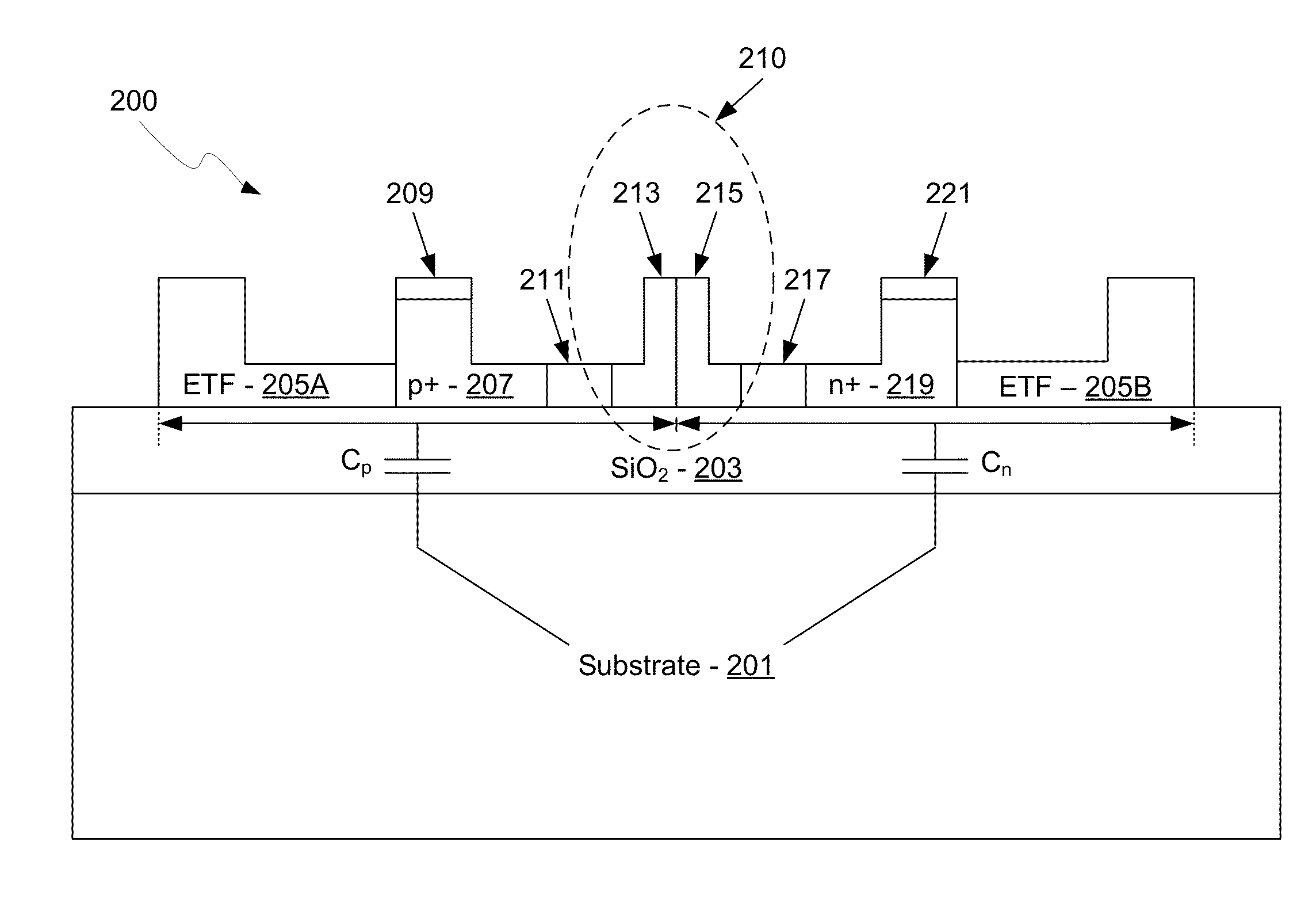
[0015]Certain aspects of the invention may be found in a method and system for a low-parasitic silicon high-speed phase modulator. Exemplary aspects of the invention may comprise fabricating an optical phase modulator that comprises a PN junction waveguide formed in a silicon layer wherein the silicon layer may be on an oxide layer and the oxide layer may be on a silicon substrate. The PN junction waveguide may have p-doped and n-doped regions on opposite sides along a length of the PN junction waveguide, and portions of the p-doped and n-doped regions may be removed. Contacts may be formed on remaining portions of the p-doped and n-doped regions. Portions of the p-doped and n-doped regions may be removed symmetrically about the PN junction waveguide. Portions of the p-doped and n-doped regions may be removed in a staggered fashion along the length of the PN junction waveguide. Etch transition features may be removed along the p-doped and n-doped regions, wherein the etch transition...


PUM


Abstract

Methods and systems for a low-parasitic silicon high-speed phase modulator are disclosed and may include fabricating an optical phase modulator that comprises a PN junction waveguide formed in a silicon layer, wherein the silicon layer may be on an oxide layer and the oxide layer may be on a silicon substrate. The PN junction waveguide may have p-doped and n-doped regions on opposite sides along a length of the PN junction waveguide, and portions of the p-doped and n-doped regions may be removed. Contacts may be formed on remaining portions of the p-doped and n-doped regions. Portions of the p-doped and n-doped regions may be removed symmetrically about the PN junction waveguide. Portions of the p-doped and n-doped regions may be removed in a staggered fashion along the length of the PN junction waveguide. Etch transition features may be removed along the p-doped and n-doped regions.

Description

CROSS-REFERENCE TO RELATED APPLICATIONS / INCORPORATION BY REFERENCE[0001]This application claims priority to U.S. Provisional Application 61 / 797,697, filed on Dec. 13, 2012, which is hereby incorporated herein by reference in its entirety.FIELD[0002]Certain embodiments of the invention relate to semiconductor processing. More specifically, certain embodiments of the invention relate to a method and system for a low-parasitic silicon high-speed phase modulator.BACKGROUND[0003]As data networks scale to meet ever-increasing bandwidth requirements, the shortcomings of copper data channels are becoming apparent. Signal attenuation and crosstalk due to radiated electromagnetic energy are the main impediments encountered by designers of such systems. They can be mitigated to some extent with equalization, coding, and shielding, but these techniques require considerable power, complexity, and cable bulk penalties while offering only modest improvements in reach and very limited scalability. ...

Claims


Application Information

Patent Timeline
IPC IPC(8): G02F1/025G02F1/225
CPCG02F1/025G02F2001/212G02F1/2257G02F2201/06G02F2202/105G02F1/212
Inventor AYAZI, ALIMASINI, GIANLORENZOSAHNI, SUBALMEKIS, ATTILAPINGUET, THIERRY
Owner CISCO TECH INC
Why Eureka
Try Eureka