
Interconnecting conduction structure for electrically connecting conductive traces of flexible circuit boards

Active Publication Date: 2015-11-12
ADVANCED FLEXIBLE CIRCUITS
View PDF15 Cites 23 Cited by
  • Summary
  • Abstract
  • Description
  • Claims
  • Application Information

AI Technical Summary

Benefits of technology

The present invention is about a way to connect flexible circuit boards that have conductive traces. The invention allows for the boards to be stacked and bonded, and the traces to be electrically connected. This helps with the increasing need for more signal transmission lines, smaller line widths, and increased power consumption. It also provides a solution for larger grounding traces. Overall, the invention allows for a more efficient and compact connection solution for flexible circuit boards.

Problems solved by technology

With the attention being paid to the number and conductive trace width of signal transmission lines, there is another concern that the power consumption of the modern electronic devices is also getting increased.
The above-mentioned solutions that arc conventionally adopted by the manufacturers do not meet the needs discussed above.
It is thus a challenge of the manufacturers of the related fields to provide a structure of a flexible circuit board that meets the above discussed needs.

Method used


Image

  • Interconnecting conduction structure for electrically connecting conductive traces of flexible circuit boards
  • Interconnecting conduction structure for electrically connecting conductive traces of flexible circuit boards
  • Interconnecting conduction structure for electrically connecting conductive traces of flexible circuit boards

Examples


Embodiment Construction

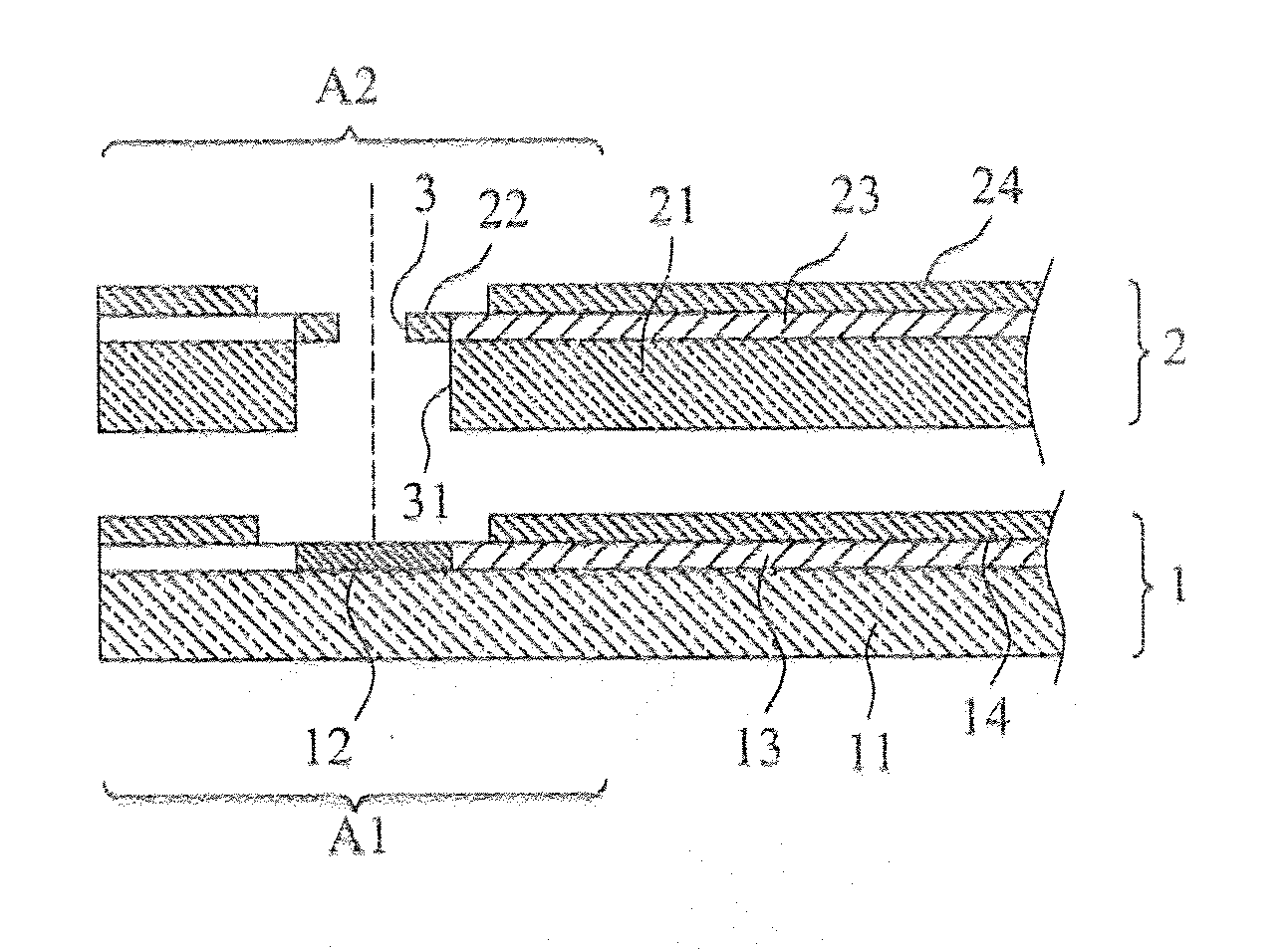
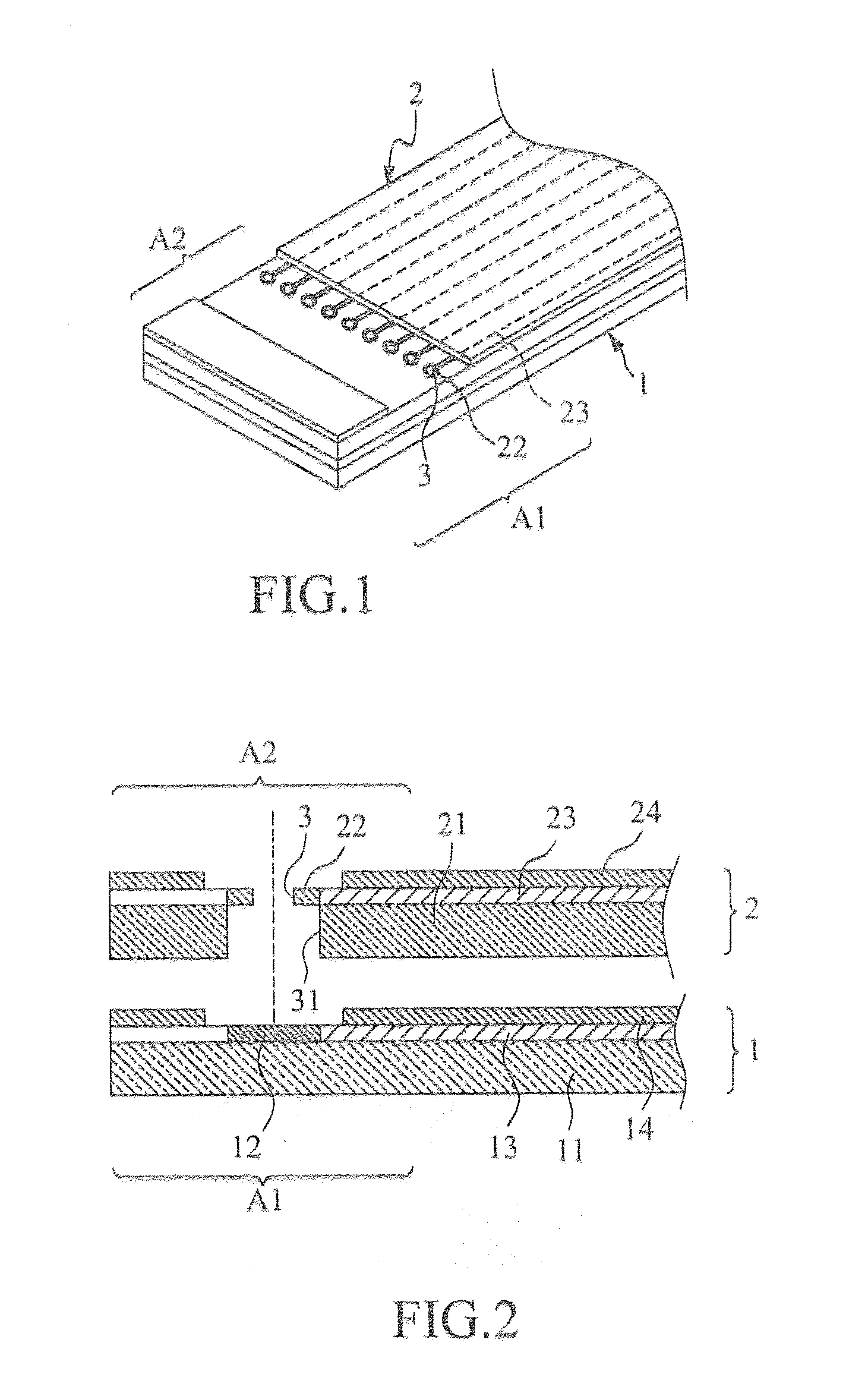
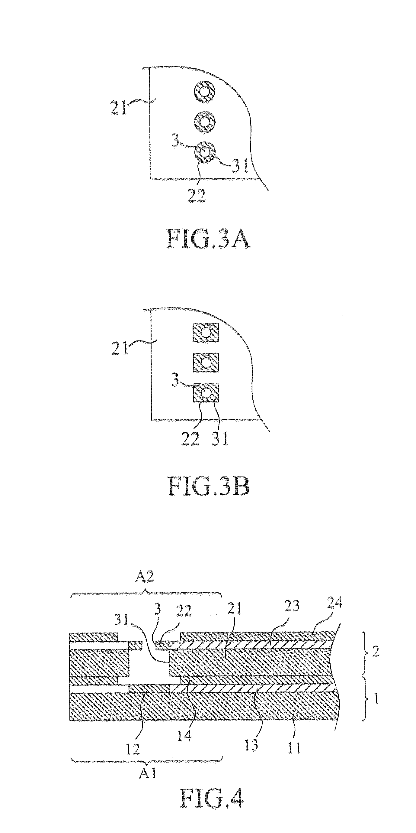
[0030]With reference to the drawings, FIG. 1 is a perspective view showing a first embodiment according to the present invention, where a first flexible circuit board 1 and a second flexible circuit board 2 are stacked and bonded to each other to form a lapped flexible circuit board; and FIG. 2 is a cross-sectional view showing the first embodiment of the present invention, with the first flexible circuit board and the second flexible circuit board being detached from each other.

[0031]As shown in the drawings, a first flexible circuit board 1 comprises a first substrate 11. The first substrate 11 defines a first stacking section A1 and comprises at least one first solder pad 12 formed in the first stacking section A1. In the instant embodiment, the first flexible circuit board 1 is a single-sided board.

[0032]The first solder pad 12 of the first flexible circuit board 1 is electrically connected to at least one first conductive trace 13 laid on the first substrate 11. The first condu...


PUM


Abstract

An interconnecting conduction structure for electrically connecting conductive traces of a lapped flexible circuit board is disclosed. The lapped flexible circuit board includes a first flexible circuit board and a second flexible circuit board. A through hole is formed in the second flexible circuit board and an interconnecting conduction member is filled in the through hole of the second flexible circuit board. The interconnecting conduction member is electrically connected to a second solder pad of the second flexible circuit board and a first solder pad of the first flexible circuit board in order to formed a lapped connection between conductive traces of the first flexible circuit board and the second flexible circuit board.

Description

BACKGROUND OF THE INVENTION[0001]1. Field of the Invention[0002]The present invention relates to a structure of flexible circuit boards, and in particular to an interconnecting conduction structure for electrically connecting conductive traces of a lapped flexible circuit board in which at least two flexible-circuit boards are stacked and an interconnecting conduction is formed there between.[0003]2. The Related Arts[0004]Flexible circuit boards have been widely used in various electronic products, particularly thin and light-weighted electronic products. For example, consumer electronic devices, such as mobile phones, digital cameras, computer peripheral devices, flat display devices, and game machines, are the commonly known applications of the flexible circuit boards.[0005]The amount of data transmitted through signal transmission lines of the electronic devices is increasingly expanded and thus, the necessary number of the signal transmission lines is also increased. To suit the...

Claims


Application Information

Patent Timeline
IPC IPC(8): H05K1/11H05K1/14
CPCH05K1/113H05K1/144H05K1/118H05K1/0215H05K2201/058
Inventor SU, KUO-FULIN, GWUN-JIN
Owner ADVANCED FLEXIBLE CIRCUITS
Learn More