
Touch panel and production method thereof

a technology of touch panel and capacitance change, applied in the field of touch panel, can solve the problems of difficult to sensitively detect the size of the screen of recent electronic devices has increased, etc., and achieve the effect of sensitively detecting a change in capacitan

Active Publication Date: 2015-11-26
JAPAN AVIATION ELECTRONICS IND LTD
View PDF2 Cites 4 Cited by
  • Summary
  • Abstract
  • Description
  • Claims
  • Application Information

AI Technical Summary

Benefits of technology

The present invention aims to provide a touch panel that can sensitively detect a change in capacitance without needing to mask the region where lead-out wiring is located. This will solve the problem associated with conventional touch panels that require masked areas for lead-out wiring.

Problems solved by technology

In particular, screens of recent electronic devices have been increasing in size.
Since a typical material used for the transparent electrode such as Indium Tin Oxide (ITO) however has a higher electric resistivity than a metal wiring, it would become difficult to sensitively detect a change in capacitance.

Method used


Image

  • Touch panel and production method thereof
  • Touch panel and production method thereof
  • Touch panel and production method thereof

Examples


embodiment 1

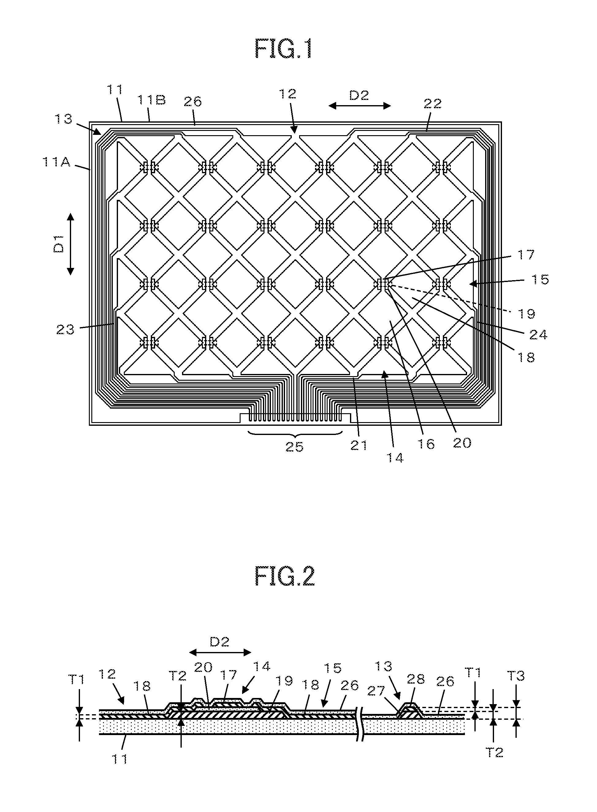
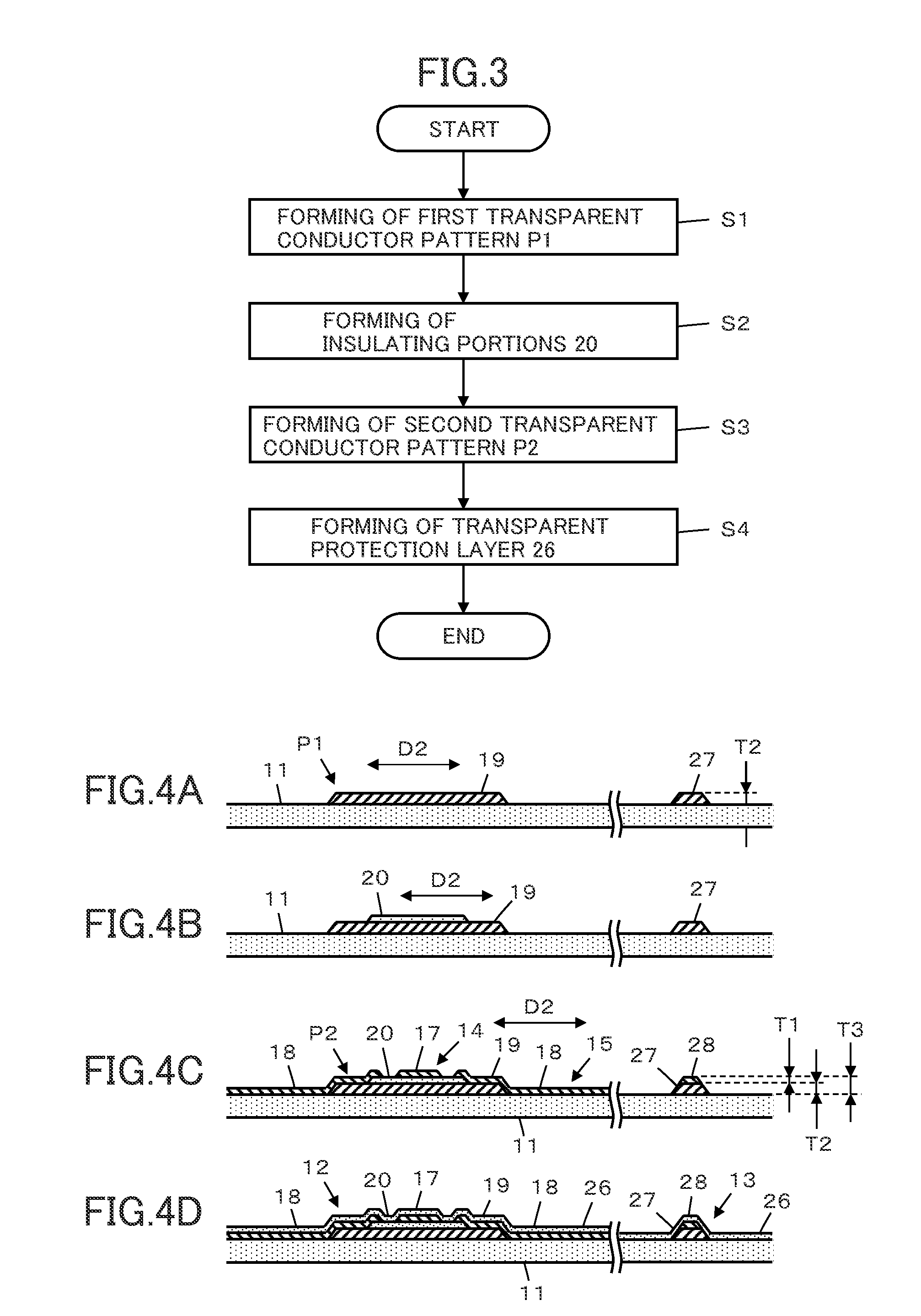
[0043]FIG. 1 illustrates a configuration of a touch panel according to Embodiment 1 of the present invention. The touch panel includes a transparent substrate 11 having a rectangular shape, a sensor electrode portion 12 formed on a surface of the transparent substrate 11, and a lead-out wiring portion 13 formed around the sensor electrode portion 12 on the surface of the transparent substrate 11.

[0044]The sensor electrode portion 12 includes a plurality of first sensor electrode arrays 14, extending along a first direction D1 and arranged parallel to one another along a second direction D2, and a plurality of second sensor electrode arrays 15, extending along the second direction D2 and arranged parallel to one another along the first direction D1, the first direction D1 being in parallel with a short side portion 11A of the rectangular transparent substrate 11, whereas the second direction D2 being in parallel with a long side portion 11B of the transparent substrate 11, i.e., orth...

embodiment 2

[0077]A touch panel according to Embodiment 2 is illustrated in FIG. 8. In the touch panel, a sensor electrode portion 12 and a lead-out wiring portion 33 are formed on a transparent substrate 31. Although not shown, a transparent protection layer is formed over the sensor electrode portion 12 and the lead-out wiring portion 33, similarly to the touch panel according to Embodiment 1.

[0078]The sensor electrode portion 12 is same as the sensor electrode portion 12 used in the touch panel according to Embodiment 1.

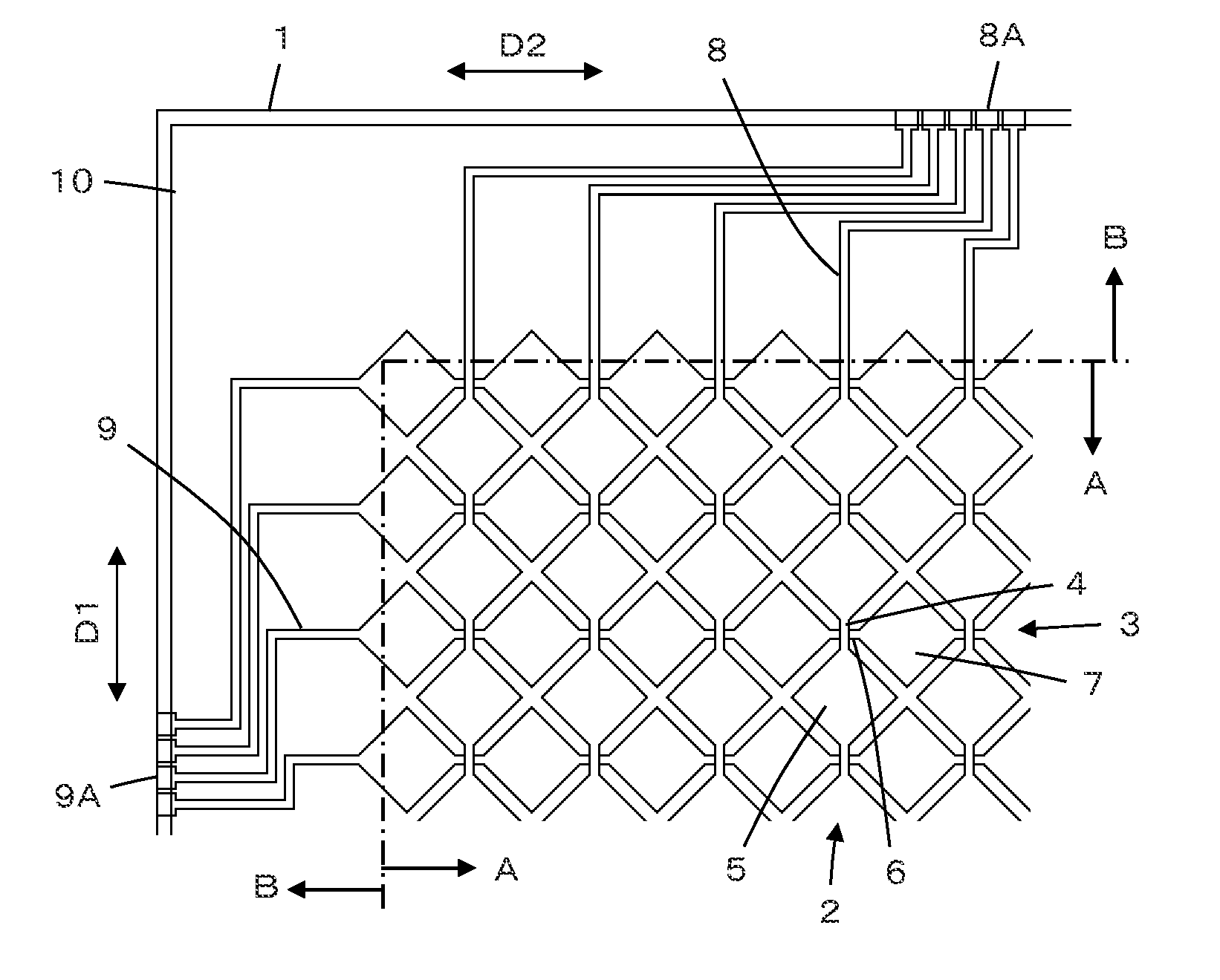
[0079]The lead-out wiring portion 33 includes a first wiring portion 21 connected to one end of each of first sensor electrode arrays 14 extending along a first direction D1 and a second wiring portion 23 connected to one end of each of second sensor electrode arrays 15 extending along a second direction D2, and the first wiring portion 21 and the second wiring portion 23 run to reach a terminal region 25.

[0080]A plurality of first island-shaped electrode portions 16 of each ...

embodiment 3

[0083]In the touch panel according to Embodiment 1, a single sensor electrode portion 12 and a single lead-out wiring portion 13 are formed on the transparent substrate 11. However, two sensor electrode portions 12 and two lead-out wiring portions 13 corresponding to the two sensor electrode portions 12 can be formed on a single transparent substrate 41 as illustrated in FIG. 9.

[0084]While a part of the lead-out wiring portion 13 is arranged between the two sensor electrode portions 12, as the lead-out wiring portion 13 is formed of the third transparent conductor layer, the part between the two sensor electrode portions 12 does not need to be masked, and the entire area of the transparent substrate 41 can be a display region of a display device to be used in combination with a touch panel.

[0085]On the other hand, in a conventional touch panel using a metal wiring, the metal wiring could not be arranged between two sensor electrode portions 12 since any opaque part should not be for...


PUM

PropertyMeasurementUnit
transparentaaaaaaaaaa
thicknessaaaaaaaaaa
transmittanceaaaaaaaaaa

Abstract

A touch panel includes first sensor electrode arrays in which first island-shaped electrode portions are arrayed along a first direction and connected through connecting portions, second sensor electrode arrays in which second island-shaped electrode portions are arrayed at intervals along a second direction, jumper wiring portions being superimposed through insulating portions and connecting the second island-shaped electrode portions arranged adjacent to each other along the second direction, and a lead-out wiring portion connected to the first and second sensor electrode arrays, the first and second sensor electrode arrays being formed of a first transparent conductor layer having a first thickness, the jumper wiring portions being formed of a second transparent conductor layer having a second thickness, the lead-out wiring portion being formed of a third transparent conductor layer having a third thickness that is larger than the first thickness.

Description

BACKGROUND OF THE INVENTION[0001]The present invention relates to a touch panel and a production method thereof, in particular, to a configuration and a production method of a capacitive touch panel.[0002]Recently, the use of a touch panel which is used in combination with a display device such as a liquid crystal display device for an input operation to an electronic device through contact with a screen has been spreading in various electronic devices including portable information equipment, vending machines, automated teller machines and gaming devices.[0003]The touch panel is categorized into several types including resistive film type, capacitive type, infrared type, ultrasonic type and electromagnetic-induction coupling type, depending on the operating principle thereof. Among those, the touch panel of the capacitive type having a high transmittance and excellent durability has been particularly attracting attention.[0004]An example of the touch panel as illustrated in FIG. 12...

Claims


Application Information

Patent Timeline
Patent Type & Authority Applications(United States)
IPC IPC(8): G06F3/041G06F3/047G06F3/044
CPCG06F3/0412G06F3/044G06F3/047Y10T29/49163G06F2203/04112G06F2203/04113G06F2203/04111G06F2203/04101G06F3/0443G06F3/0446G06F2203/04103
Inventor MATSUMOTO, KENJIOHGUSHI, TSUTOMUTAKIGUCHI, TSUYOSHIAKIZUKI, JOJI
Owner JAPAN AVIATION ELECTRONICS IND LTD
Learn More