Semiconductor memory device, a memory module including the same, and a memory system including the same

a memory module and memory technology, applied in the field of semiconductor memory devices, can solve the problems of high speed and low power requirements, and achieve the effect of reducing the number of memory devices

Active Publication Date: 2015-12-03
SAMSUNG ELECTRONICS CO LTD
View PDF5 Cites 33 Cited by
  • Summary
  • Abstract
  • Description
  • Claims
  • Application Information

AI Technical Summary

Benefits of technology

The patent describes a semiconductor memory device that includes an output driver and a ZQ calibration unit to generate a pull-up VOH code and a pull-down VOH code based on a control code. The resistance of the pull-up driver and the pull-down driver is determined based on the resistance of an ODT resistor of a memory controller. The ratio between the power supply voltage and the VOH is determined based on the resistance of the ODT resistor. The output driver generates a current based on the pull-up VOH code and the pull-down VOH code to determine the voltage at a first node. The semiconductor memory device may include a pre-driver and a selection circuit to select the appropriate target VOH code. The technical effect of this patent is to provide a semiconductor memory device that can calibrate the VOH code to improve the accuracy of the data signal and the reliability of the memory system.

Problems solved by technology

However, low power and high speed are typical requirements for semiconductor memory devices used in a mobile environment.

Method used


Image

  • Semiconductor memory device, a memory module including the same, and a memory system including the same
  • Semiconductor memory device, a memory module including the same, and a memory system including the same
  • Semiconductor memory device, a memory module including the same, and a memory system including the same

Examples


Embodiment Construction

[0053]The inventive concept now will be described more fully hereinafter with reference to the accompanying drawings, in which exemplary embodiments are shown. This inventive concept may, however, be embodied in many different forms and should not be construed as limited to the embodiments set forth herein. In the drawings, the size and relative sizes of layers and regions may be exaggerated for clarity. Like numbers may refer to like elements throughout the application.

[0054]It will be understood that when an element is referred to as being “connected” or “coupled” to another element, it can be directly connected or coupled to the other element or intervening elements may be present.

[0055]As used herein, the singular forms “a”, “an” and “the” are intended to include the plural forms as well, unless the context clearly indicates otherwise.

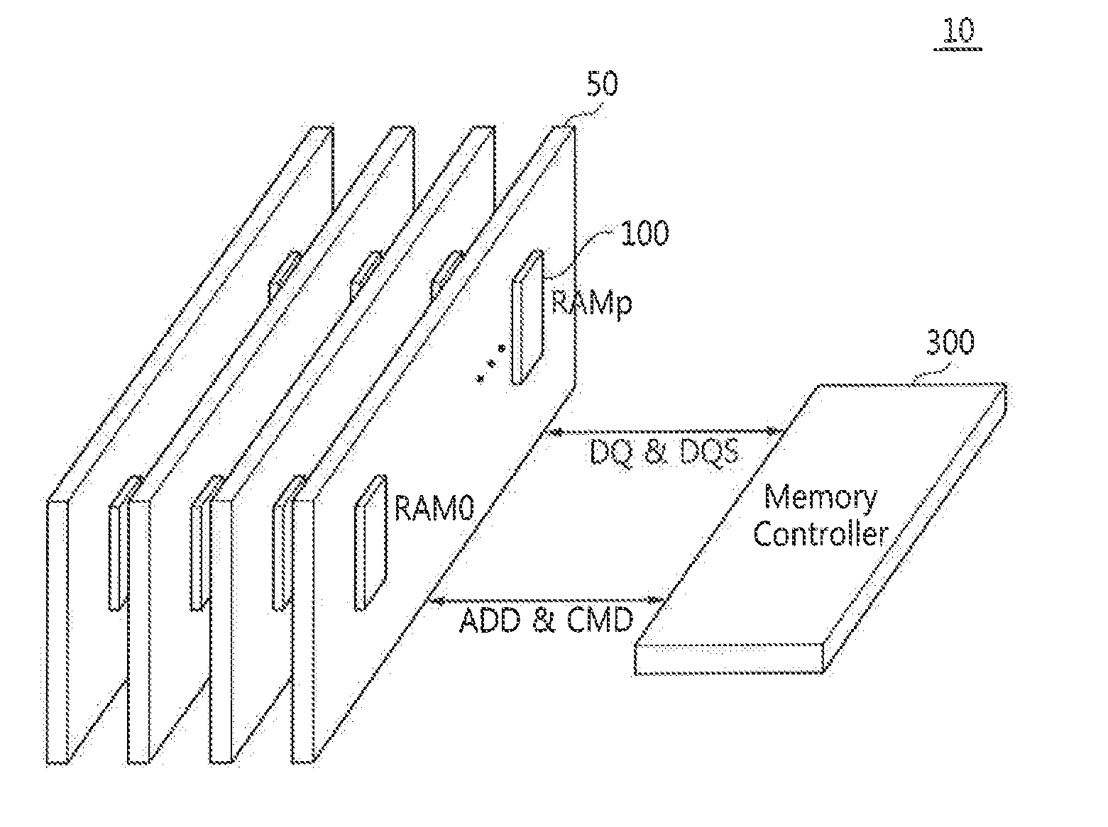
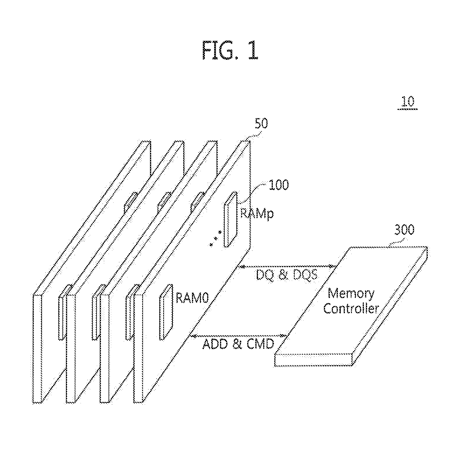
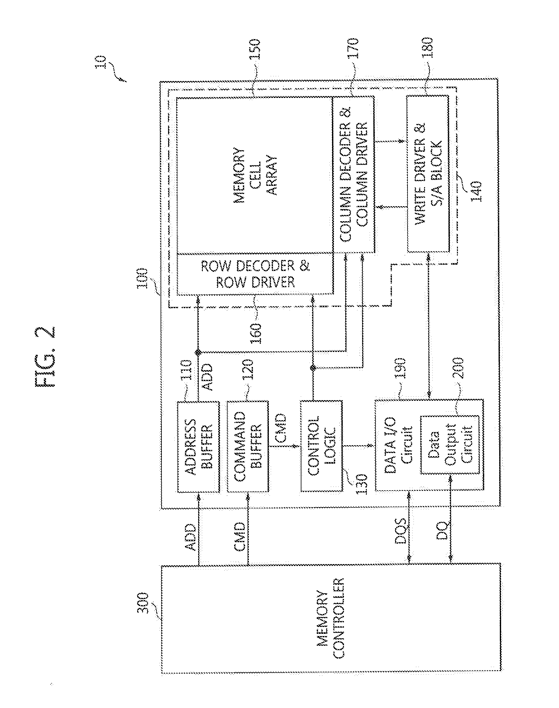
[0056]FIG. 1 is a schematic diagram of a memory system 10 according to an exemplary embodiment of the inventive concept. The memory system 10 may ...


PUM


Abstract

A semiconductor memory device includes a ZQ calibration unit configured to generate a pull-up VOH code according to a first target VOH proportional to a power supply voltage and an output driver configured to generate a data signal having a VOH proportional to the power supply voltage based on the pull-up VOH code, wherein VOH means “output high level voltage.”

Description

CROSS-REFERENCE TO RELATED APPLICATION[0001]This application claims priority under 35 U.S.C, §119 to Korean Patent Application No. 10-2014-0065149 filed on May 29, 2014, the disclosure of which is incorporated by reference herein in its entirety.TECHNICAL FIELD [0002]Exemplary embodiments of the inventive concept relate to a semiconductor memory device, a memory module including the same, and a memory system including the same, and more particularly, to a semiconductor memory device for reducing noise in a data signal thereof a memory module including the same, and a memory system including the same.DISCUSSION OF RELATED ART [0003]A semiconductor memory device may exchange commands and data with an external system, e.g., a memory controller. When impedance of a bus line connecting the semiconductor memory device and the external system is different from that of a signal line directly connected with the bus line within the semiconductor memory device, signal reflection may occur. To ...

Claims


Application Information

Patent Timeline
Patent Type & Authority Applications(United States)
IPC IPC(8): G11C7/12H03K19/00
CPCH03K19/0005G11C7/12G11C5/147G11C7/1057G11C29/021G11C29/022G11C29/028G11C29/50008G11C2207/2254
Inventor LEE, KI WONBAE, SEUNG JUNPARK, JOON YOUNGBAE, YONG CHEOL
Owner SAMSUNG ELECTRONICS CO LTD
Why Eureka
Try Eureka