Gate driving circuit on liquid crystal panel

A technology for gate driving circuits and driving transistors, which can be used in instruments, static indicators, etc., to solve problems such as high power, complicated circuit design and fabrication, and high-level voltage Vlog attenuation.

Active Publication Date: 2011-03-30
AU OPTRONICS CORP
View PDF3 Cites 5 Cited by
  • Summary
  • Abstract
  • Description
  • Claims
  • Application Information

AI Technical Summary

Problems solved by technology

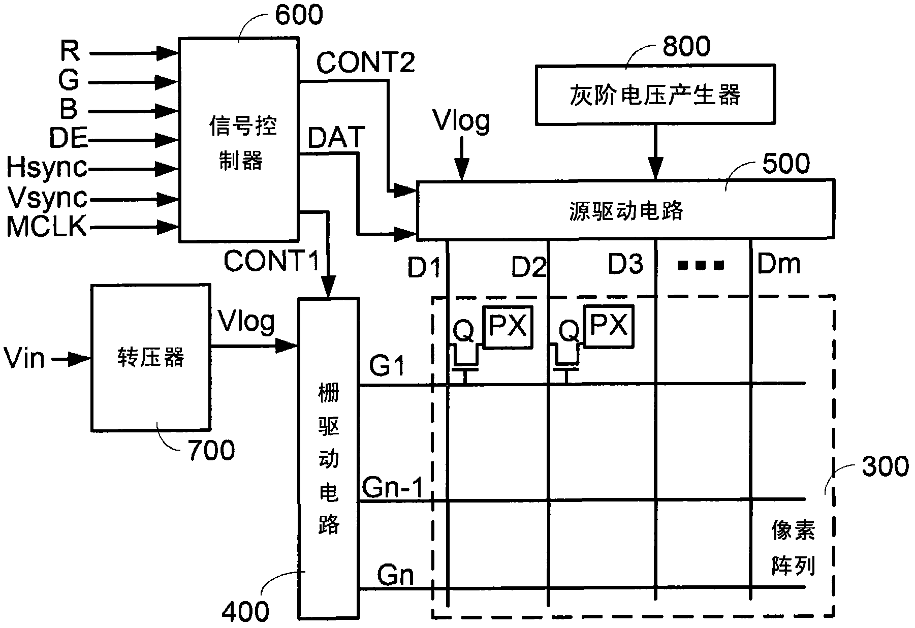
[0009] Figure 2 with figure 1 It has the same disadvantage, that is, the operating voltages of the gate drive circuit 400 and the source drive circuit 500 are both the higher high-level voltage Vlog output by the converter 710, so the consumed power (P=f×C×V 2 ) will be larger
[0010] Furthermore, after the higher high-level voltage Vlog is output by the transformer 700, it must go through a layout trace before being input into the gate driving circuit 400 and the source driving circuit 500, therefore, a higher high-level voltage will be caused. The bit voltage Vlog attenuates and affects the quality of the signal (for example, the output waveform of the gate drive signal is distorted)
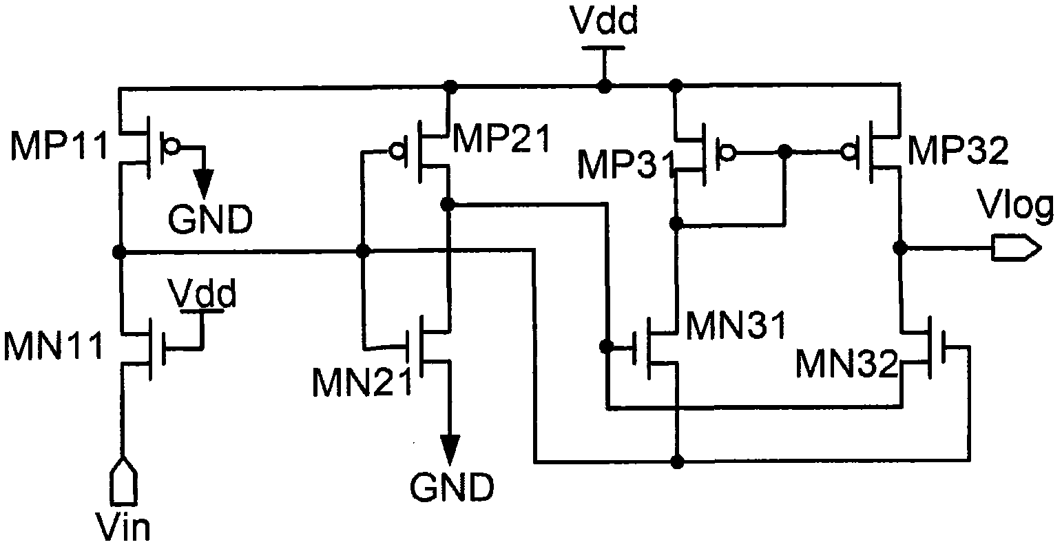
[0011] Furthermore, the existing converter must use both N-type transistors and P-type transistors, which will complicate the design and manufacture of the circuit

Method used


Image

  • Gate driving circuit on liquid crystal panel
  • Gate driving circuit on liquid crystal panel
  • Gate driving circuit on liquid crystal panel

Examples


no. 1 example

[0052] According to the first embodiment of the present invention, the shift register in the gate drive circuit integrates the shift unit 910 and the transformer 920, and the transformer is located in the last stage of the gate drive circuit, so it can effectively Power loss is reduced, and distortion of gate drive signals is prevented. Furthermore, the transistors in the present invention are all N-type thin film variable crystals of the same type, so the design and manufacture of the gate driving circuit can be greatly simplified.

[0053] Please refer to Image 6 , which shows the second embodiment of the gate driving circuit on the GOA panel of the present invention. The gate driving circuit 950 includes a plurality of shift registers 951˜95n+1. The first shift register 951 generates a first gate driving signal G1 and a first secondary notification signal NS1 after receiving the start signal START. After receiving the first secondary notification signal NS1 , the second...


PUM


Abstract

The invention discloses a gate driving circuit on a liquid crystal panel. The gate driving circuit comprises a plurality of shift registers, wherein the nth shift register comprises a shift unit and a voltage converter; the shift unit can generate an nth secondary notice signal and an nth gate driving signal according to an (n-1)th secondary notice signal output by the (n-1)th shift register; and the high level of the nth gate driving signal is provided by the voltage converter and is greater than that of the nth secondary notice signal.

Description

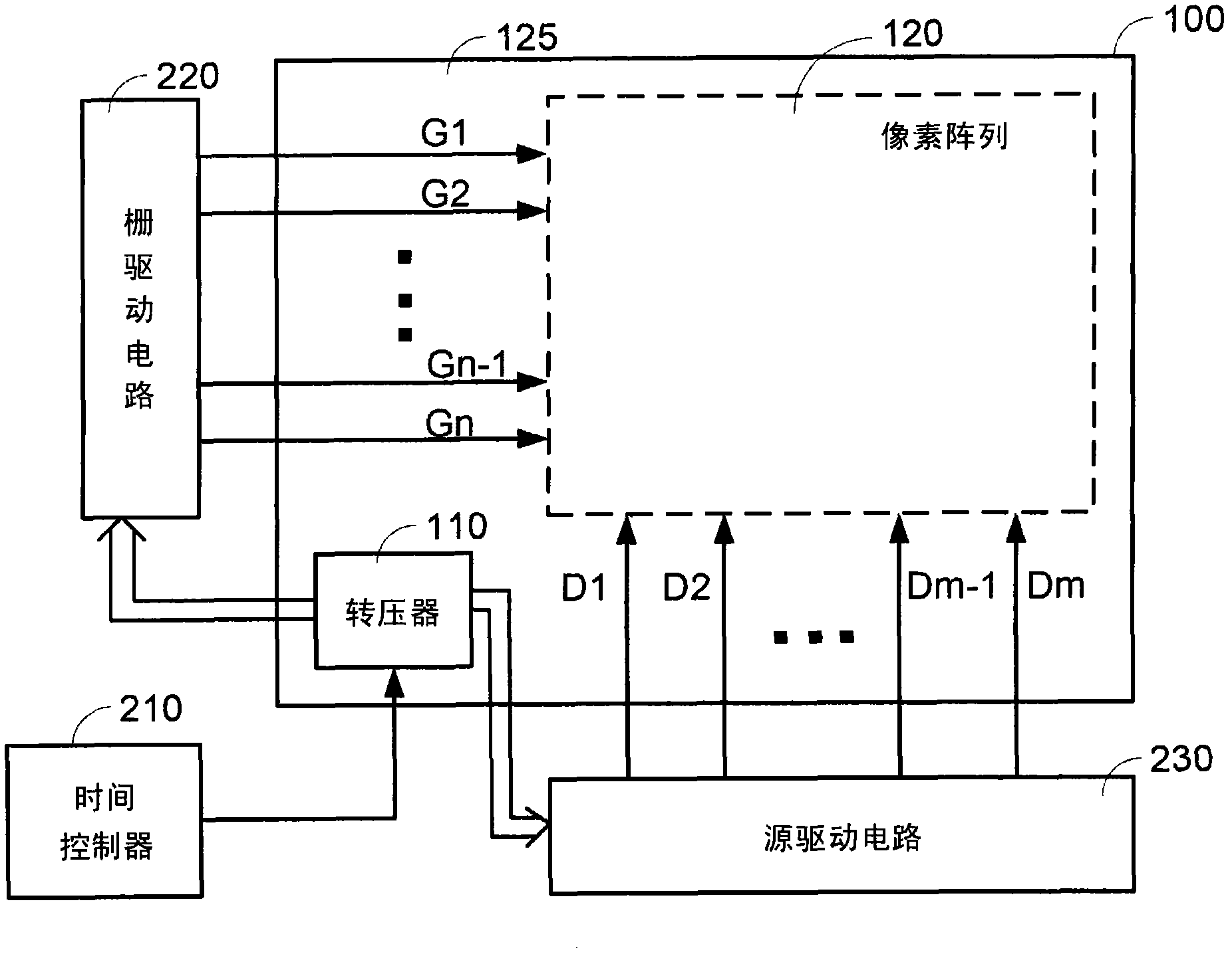
【Technical field】 [0001] The present invention relates to a gate drive circuit on a liquid crystal panel, in particular to a gate drive circuit combined with a shift register and a level shifter applied to a liquid crystal panel. 【Background technique】 [0002] Please refer to figure 1 , which is a schematic diagram of an existing liquid crystal panel and its related control circuit. In general, the liquid crystal panel 100 includes a visible area 120 and an invisible area (the area outside the dotted line) 125 . The visible area 120 includes a pixel array (pixel array), and the pixel array includes a plurality of gate lines (G1-Gn) and a plurality of data lines (D1-Dm). Furthermore, the gate lines ( G1 -Gn) can be sequentially connected to the gate driving circuit 220 via the wiring in the invisible region 125 . Similarly, the data lines ( D1 ˜ Dm ) are also sequentially connected to the source driving circuit (source driving circuit) 230 . [0003] Furthermore, the liq...

Claims


Application Information

Patent Timeline
Patent Type & Authority Applications(China)
IPC IPC(8): G09G3/36
Inventor 赖威任
Owner AU OPTRONICS CORP
Why Eureka
Try Eureka