Semiconductor device, module, and electronic device including a conversion circuit having a second switch rendered conductive together with a first switch

a technology of semiconductor devices and electronic devices, applied in the direction of radio frequency controlled devices, pulse techniques, instruments, etc., can solve problems such as degradation of the resolution of reproduced images, and achieve the effect of improving the electrical breakdown voltage and stable operation

Inactive Publication Date: 2009-10-27
ROHM CO LTD
View PDF7 Cites 150 Cited by
  • Summary
  • Abstract
  • Description
  • Claims
  • Application Information

AI Technical Summary

Benefits of technology

[0046]According to the semiconductor device of the present invention, the electrostatic breakdown voltage can be improved without affecting the operation of a conversion circuit that shifts a signal such that a reference of the signal attains the level of an externally applied input potential by providing a switch connected between the conversion circuit and an input terminal to which the input potential is applied.
[0047]According to the module and electronic device including a plurality of semiconductor devices set forth above of the present invention, stable operation can be realized.

Problems solved by technology

Such a smaller dynamic range will disallow reproduction of the tone of the original image, leading to the problem of degradation in the resolution of the reproduced image.

Method used


Image

  • Semiconductor device, module, and electronic device including a conversion circuit having a second switch rendered conductive together with a first switch
  • Semiconductor device, module, and electronic device including a conversion circuit having a second switch rendered conductive together with a first switch
  • Semiconductor device, module, and electronic device including a conversion circuit having a second switch rendered conductive together with a first switch

Examples


Embodiment Construction

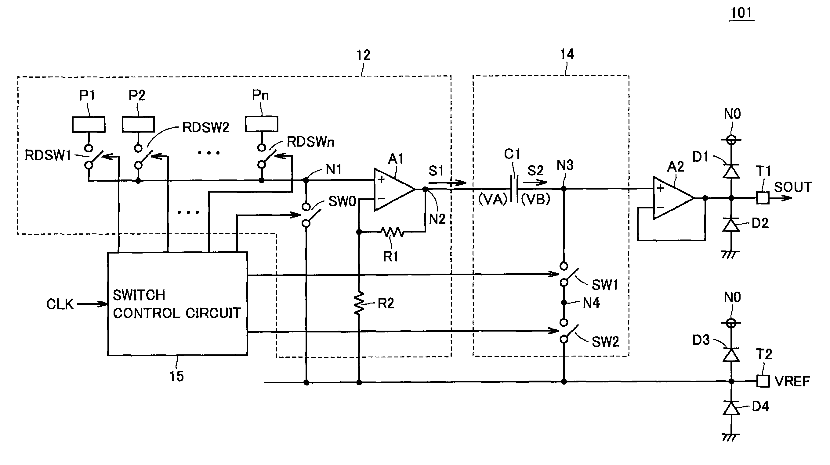
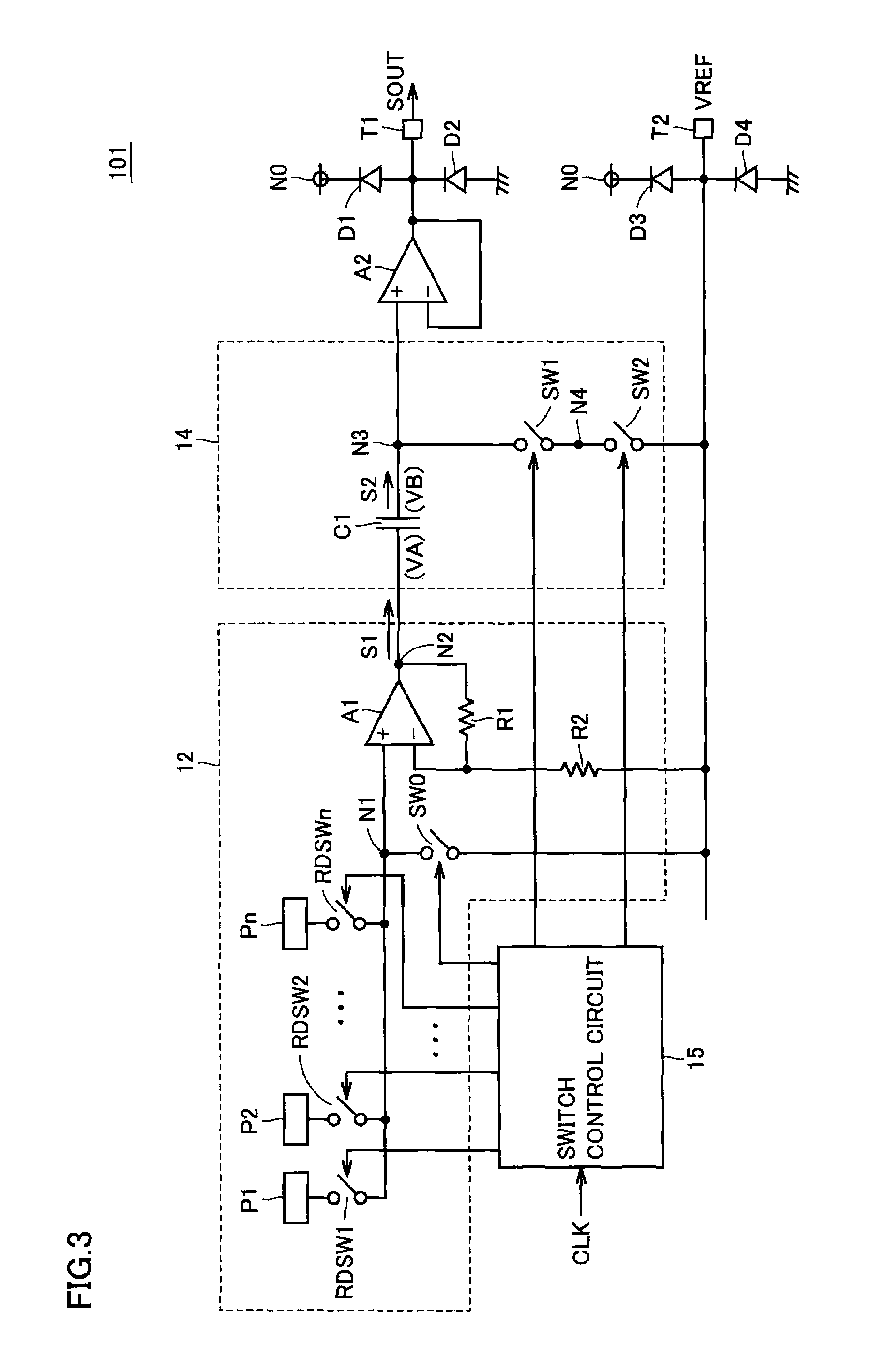
[0060]Embodiments of the present invention will be described in detail with reference to the drawings hereinafter. In the drawings, the same reference characters represent the same or corresponding elements.

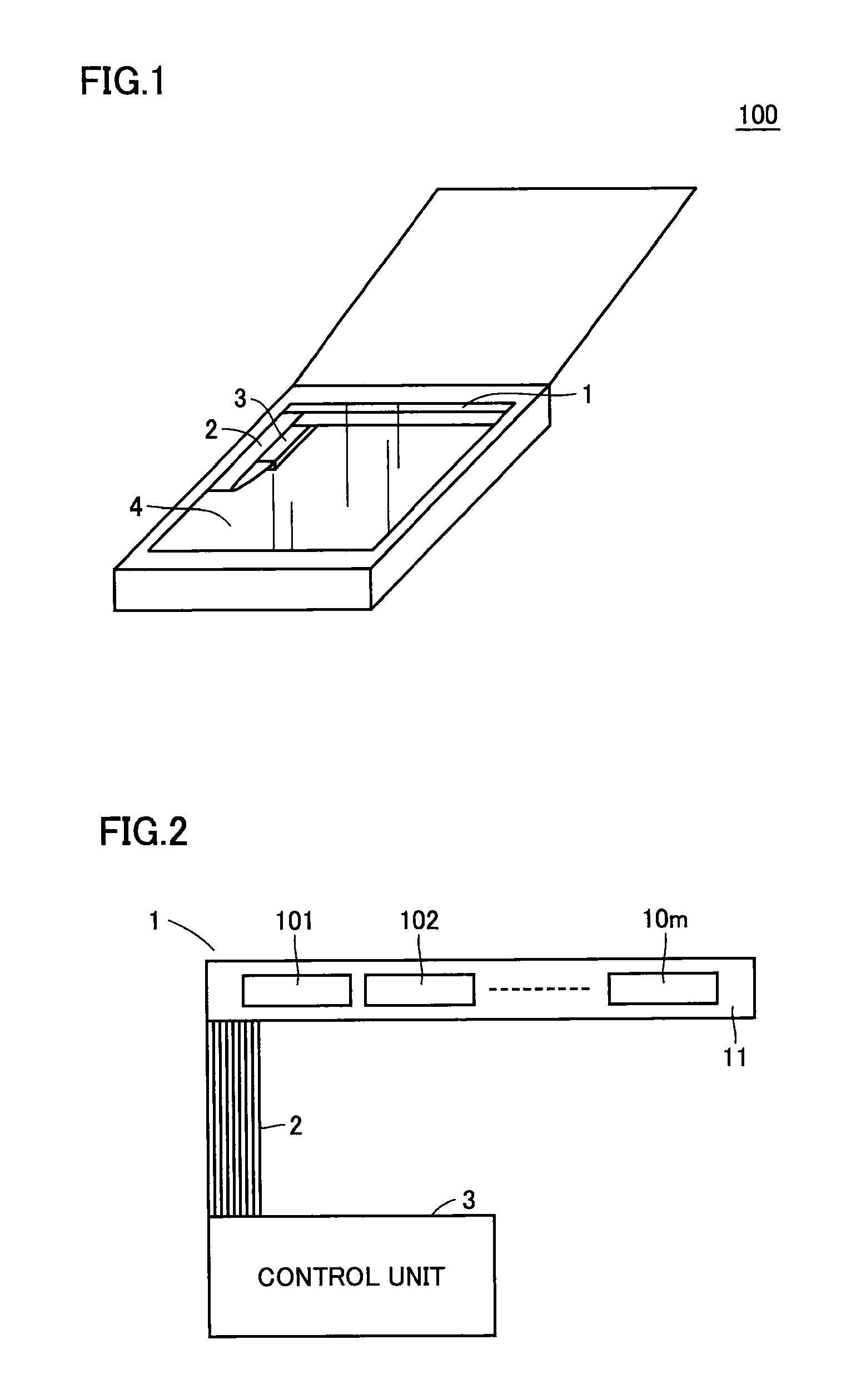
[0061]FIG. 1 represents an example of an electronic device of the present invention. Referring to FIG. 1, a scanner 100 is illustrated as an example of the electronic device of the present invention. Scanner 100 includes an image sensor head 1, a flexible cable 2 connected to image sensor head 1, a control unit 3 connected to image sensor head 1 via flexible cable 2, and glass 4 where a document on which information such as text and images are drawn is placed.

[0062]Image sensor head 1 corresponds to the module of the present invention. Image sensor head 1 is movable, and reads out the text and image from the document via glass 4 to send an image signal to control unit 3. Control unit 3 reproduces an image according to image signals.

[0063]Although scanner 100 is illustrated as a f...


PUM


Abstract

The breakdown voltage between the potential of a terminal and the ground potential (or power supply potential) is improved by increasing the gate width of an MOS transistor included in a switch. Accordingly, another switch and the like are protected even when surge is applied to the terminal. By increasing the gate width of the MOS transistor included in the switch, the size of the other switch does not have to be increased. Therefore, variation in the potential at a node occurring when the other switch attains a non-conductive state from a conductive state can be suppressed. Therefore, a semiconductor device having the electrostatic breakdown voltage improved without influence on processing carried out based on an input potential from an external source, a module including a plurality of such semiconductor devices, and an electronic device including such a module can be provided.

Description

TECHNICAL FIELD[0001]The present invention relates to a semiconductor device, a module including a plurality of semiconductor devices, and an electronic device including such a module. More specifically, the present invention relates to an image sensor IC (Integrated Circuit) employed for document reading, image input, and the like, an image sensor device including a plurality of image sensor ICs, and an electronic device including this image sensor device.BACKGROUND ART[0002]Conventionally, an image sensor device having a plurality of image sensor ICs aligned linearly to directly read out information such as characters and images on a document is used extensively in electronic devices such as facsimile apparatus, copy machines, and scanners (hereinafter, referred to as “image input device”).[0003]FIG. 9 schematically represents a basic configuration of an image sensor IC. Referring to FIG. 9, an image sensor IC 111 includes a photoelectric converter 112 converting received light in...

Claims


Application Information

Patent Timeline
Patent Type & Authority Patents(United States)
IPC IPC(8): H01J40/14H01L21/8234H01L21/8238H01L27/06H01L27/088H01L27/092H03F1/26H03F1/52H04N1/028
CPCH01L21/823456H01L27/0248H04N5/357H03K17/102H03K17/6871H01L27/092H03K2217/0018H01L27/146H04N25/60H03F1/52H01L21/8238H01L27/088H01L27/06
Inventor YAMADA, NOBUYUKI
Owner ROHM CO LTD
Why Eureka
Try Eureka