
Electrochromic devices having improved ion conducting layers

a technology of ion conducting layer and electrochromic device, which is applied in the field of solid state, inorganic thin film electrochromic device, can solve the problems of shortening the required voltage, inhibiting the flow of ions, and typically suffering from electronic leakage and electronic breakdown of devices, so as to improve the efficiency of ion conducting layer and reduce the risk of electronic leakage , the effect of increasing the voltag

Inactive Publication Date: 2009-09-22
SAGE ELECTROCHROMICS
View PDF78 Cites 153 Cited by
  • Summary
  • Abstract
  • Description
  • Claims
  • Application Information

AI Technical Summary

Benefits of technology

[0038]Applicants have found that electrochromic devices utilizing the improved ion conductor layer as disclosed herein color more deeply by virtue of the increased voltage developed across the ion conductor prior to electronic breakdown. Applicants have also found that electrochromic devices utilizing the improved ion conductor layer as disclosed herein are less susceptible to electronic leakage. Applicants have also discovered that the improved ion conductor layer contained within an electrochromic device provides thermal stabilization properties to the electrochromic device, which are desirable for more robust manufacturing.

Problems solved by technology

Such devices typically suffer from electronic leakage and electronic breakdown.
However, any electronic current that leaks or passes through the ion conductor layer serves to short out the required voltage and inhibits the flow of ions.
As such, electronic leakage current leads to compromises in device performance including a lowered dynamic range, non-uniform coloration, decreased ionic conductance, slower switching rates, and increased power consumption.
Merely increasing the thickness of the ion conductor layer may result in a reduction of leakage current, but at the expense of degraded optical properties, increased layer deposition time and cost, and reduced switching rates.
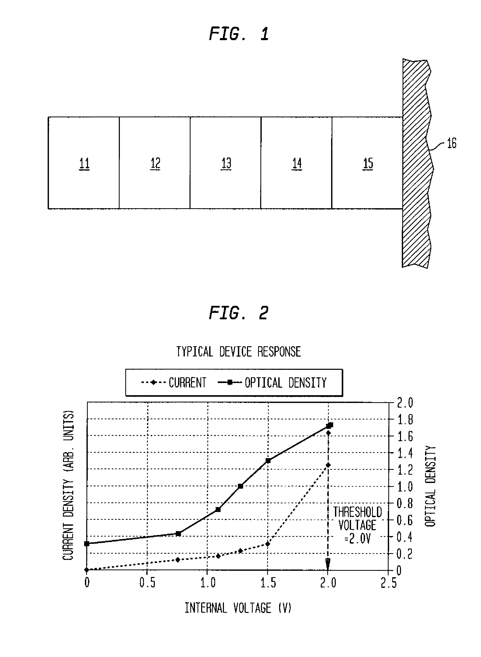
Moreover, solid state electrochromic devices are also subject to “electronic breakdown.”FIG. 2 shows the equilibrium electrical and optical characteristics of an electrochromic device for applied voltages in the ‘forward’ or coloring polarity, up until the point where substantial electronic leakage current begins to flow.
Above the threshold voltage, however, the electrochromic device breaks down electronically and any additional current flowing is primarily electronic leakage.
However, Takahashi does not teach a multi-layered thin film ion conductor layer capable of reducing electronic leakage while increasing the voltage that may be developed across the ion conductor layer.

Method used


Image

  • Electrochromic devices having improved ion conducting layers
  • Electrochromic devices having improved ion conducting layers
  • Electrochromic devices having improved ion conducting layers

Examples


Embodiment Construction

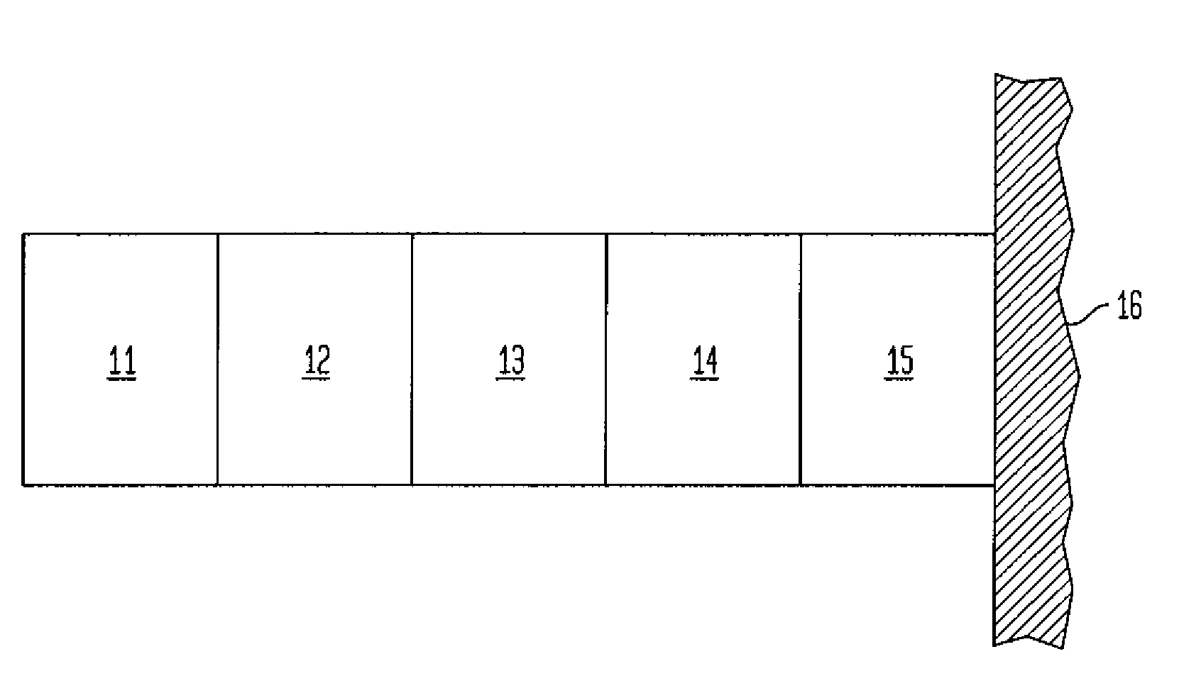
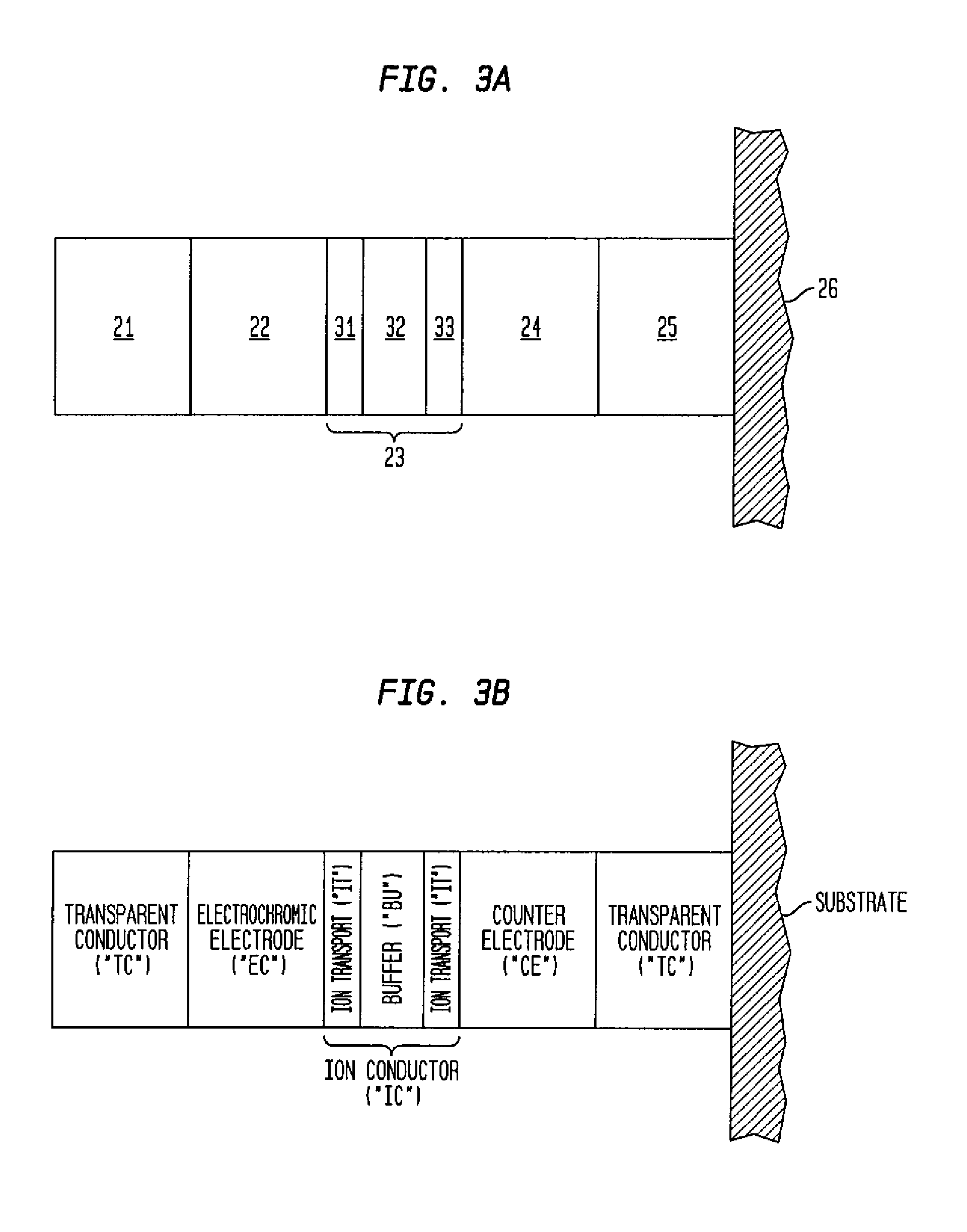
[0043]One object of the present invention is to provide an electrochromic device having an improved ion conductor layer. The improved ion conductor layer serves to block electron flow in both directions while permitting ionic conduction. The improved ion conductor layer also provides thermal stabilization properties, which are desirable for more robust processing. This and other objectives are realized by means of an electrochromic device utilizing a multi-layered thin film ion conductor comprised of thin films of at least two ion transport layers and a buffer layer, wherein the at least two ion transport layers and the buffer layer alternate within the ion conducting layer. Such a multi-layered thin film ion conductor layer allows for devices to color more deeply by increasing the voltage developed across the ion conductor prior to electronic breakdown while reducing the amount of electronic leakage.

[0044]Another objective of the present invention is to provide an ion conductor lay...


PUM

PropertyMeasurementUnit
thicknessaaaaaaaaaa
thicknessaaaaaaaaaa
thicknessaaaaaaaaaa

Abstract

An improved ion conductor layer for use in electrochromic devices and other applications is disclosed. The improved ion-conductor layer is comprised of at least two ion transport layers and a buffer layer, wherein the at least two ion transport layers and the buffer layer alternate within the ion conductor layer such that the ion transport layers are in communication with a first and a second electrode. Electrochromic devices utilizing such an improved ion conductor layer color more deeply by virtue of the increased voltage developed across the ion conductor layer prior to electronic breakdown while reducing the amount of electronic leakage. Also disclosed are methods of making electrochromic devices incorporating the improved ion conductor layer disclosed herein and methods of making ion conductors for use in other applications.

Description

[0001]This application claims the benefit of the filing date of U.S. Provisional Patent Application No. 60 / 725,581 filed Oct. 11, 2005, the disclosure of which is hereby incorporated herein by reference.BACKGROUND OF THE INVENTION[0002]The present invention relates to electrochromic devices and more particularly relates to solid-state, inorganic thin film electrochromic devices.[0003]Electrochromic materials and devices have been developed as an alternative to passive coating materials for light and heat management in building and vehicle windows. In contrast to passive coating materials, electrochromic devices employ materials capable of reversibly altering their optical properties following electrochemical oxidation and reduction in response to an applied potential. The optical modulation is the result of the simultaneous insertion and extraction of electrons and charge compensating ions in the electrochemical material lattice.[0004]In general, electrochromic devices have a compos...

Claims


Application Information

Patent Timeline
Patent Type & Authority Patents(United States)
IPC IPC(8): G02F1/15
CPCG02F1/1525G02F2201/16
Inventor BURDIS, MARK SAMUELGREER, BRYAN D.WEIR, DOUGLAS GLENN JOHN
Owner SAGE ELECTROCHROMICS
Learn More