connector

Active Publication Date: 2016-01-14
JAPAN AVIATION ELECTRONICS IND LTD
View PDF5 Cites 27 Cited by
  • Summary
  • Abstract
  • Description
  • Claims
  • Application Information

AI Technical Summary

Benefits of technology

[0006]The present invention is made to solve the above-mentioned problems in the prior art and an object thereof is to provide

Problems solved by technology

Therefore it becomes difficult to satisfactorily suppress cross-talk, only by widening the space between the signal contacts in a certain limited range.
However, for example, in a connector in which the contact arranging pitch is reduced to about 0.5 mm or l

Method used


Image

  • connector
  • connector
  • connector

Examples


embodiment 1

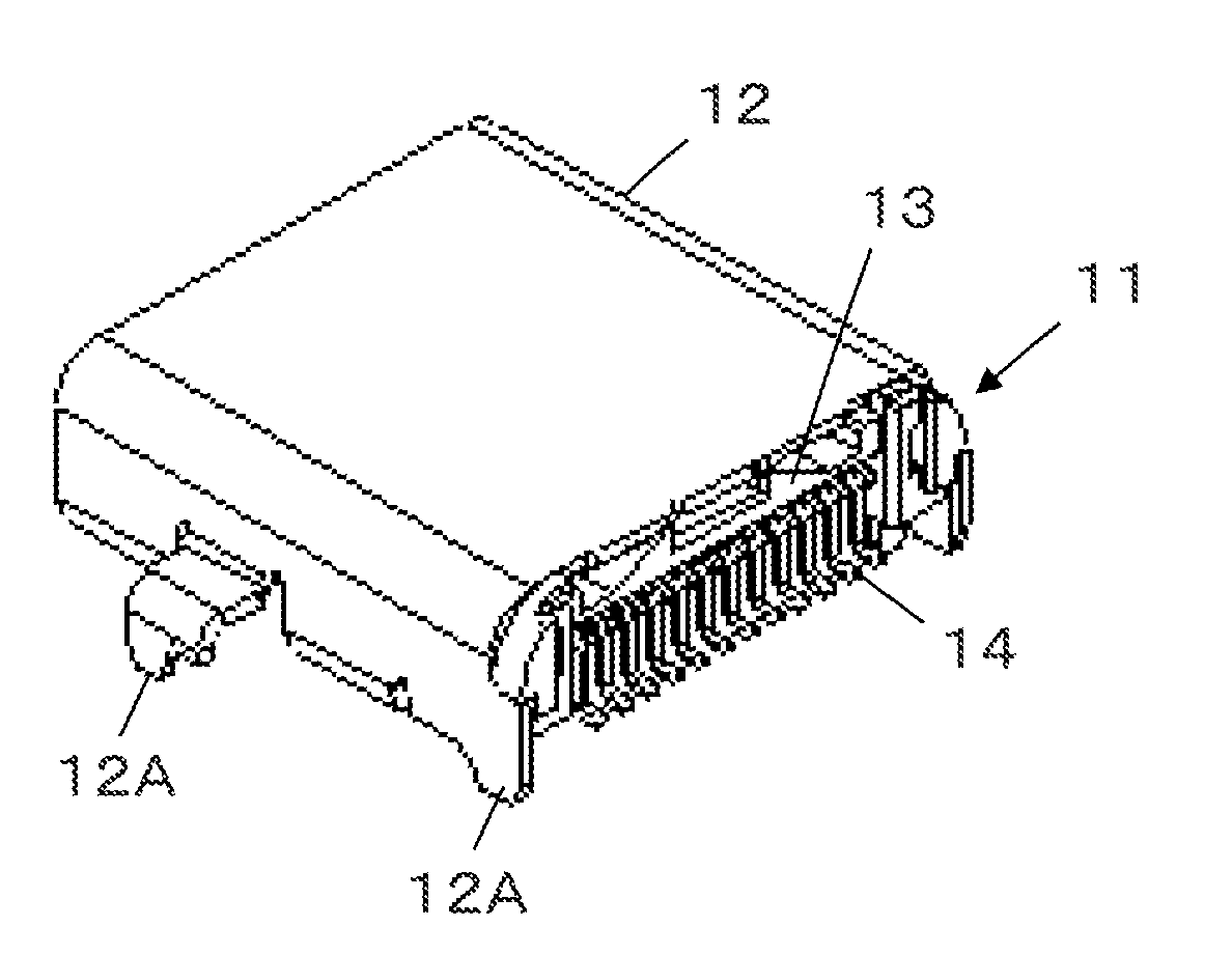
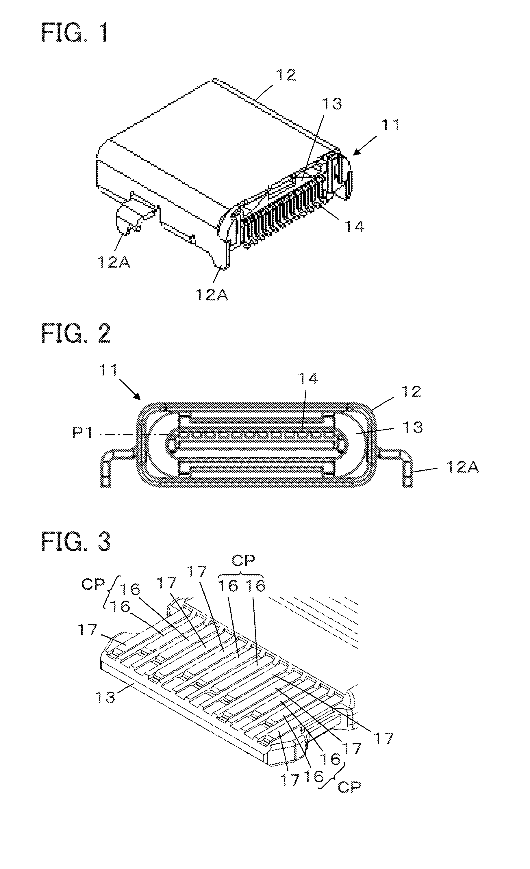
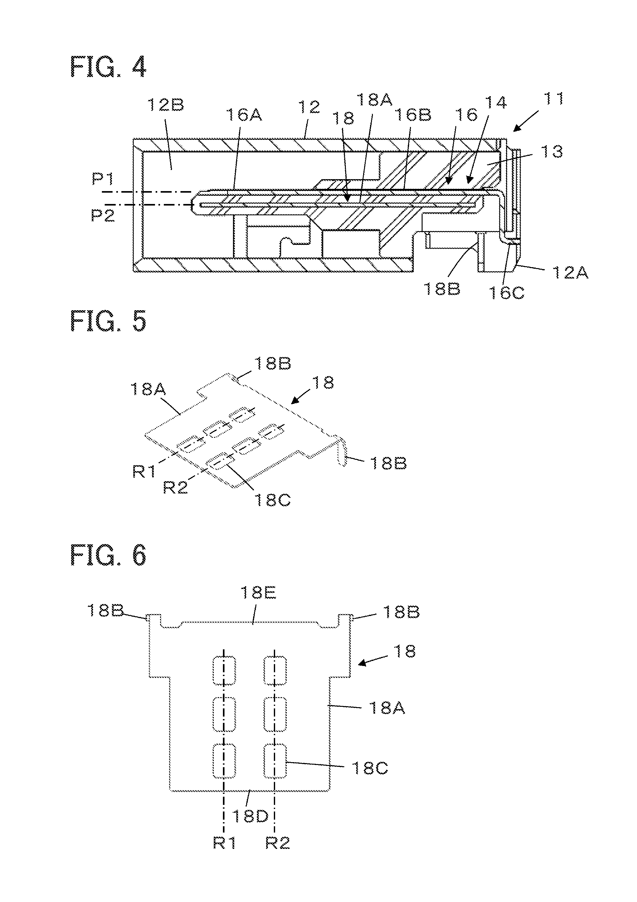
[0034]FIG. 1 shows a connector 11 according to Embodiment 1. The connector 11 is a receptacle connector to be fixed to a substrate in electronic devices such as portable devices and information devices. The connector 11 has a metal shell 12, an insulator 13 disposed inside the metal shell 12, and contacts 14 held by the insulator 13.

[0035]The metal shell 12 covers an outer periphery portion of the insulator 13, excluding a front surface section and a back surface section of the insulator 13, facing the fitting direction of the connector 11. Shell leg sections 12A to be mounted to the substrate are formed protrudingly in a direction perpendicular to the fitting direction of the connector 11.

[0036]As shown in FIG. 2, contacts 14 are held by the insulator 13, with the contacts 14 being arranged in a line on a contact array plane P1. These contacts 14 consist of signal contacts 16 configured to transmit and receive signals to and from a counter connector, and non-signal contacts 17 to b...

embodiment 2

[0054]While, in the around plate 18 used in Embodiment 1 described above, as shown in FIG. 6, the openings 18C are formed in the two rows R1 and R2 parallel to each other, and each of the rows R1 and R2 has three openings 18C between the plate front end section 18D and the plate back end section 18E, the present invention is not limited to this.

[0055]For example, as shown in FIG. 13A, a ground plate 21 having a single opening 21C that extends from a plate front end section 21D to a plate back end section 21E, corresponding to the non-signal contact 17, instead of having plural openings 21C between the plate front end section 21D and the plate back end section 21E, may be used.

[0056]Also, as in a ground plate 22 shown in FIG. 13B, the plate front end section 22D may be notched to provide an opening 22C with the front end being opened.

[0057]Further, as in a ground plate 23 shown in FIG. 13C, a plate front end section 23D and a plate back end section 23E may be both notched to provide ...

embodiment 3

[0062]FIG. 15 shows a connector 31 according to Embodiment 3. The connector 31 uses an insulator 33, instead of the insulator 13 in the connector 11 in Embodiment 1. The contacts 14 arranged on the contact array plane P1 and contacts 34 arranged on a contact array plane P3 are held by the insulator 33. The two contact array planes P1 and P3 are disposed parallel to each other, so that the contacts 14 and 34 are arranged in two rows of an upper row and a lower row, respectively.

[0063]In the insulator 33, the ground plate 18 used in Embodiment 1 is held. As shown in FIG. 16, the ground plate 18 is disposed adjacent to each of the contacts 14 and the contacts 34, and between the contacts 14 and the contacts 34.

[0064]As shown in FIG. 17, the contact array plane P1 and the contact array plane P3 are disposed at both sides of the ground plane P2 in which the plate body 18A of the ground plate 18 is disposed. The contacts 34 arranged on the contact array plane P3 are aligned symmetry to th...


PUM


Abstract

A connector includes a plurality of signal contacts and a plurality of non-signal contacts arranged on at least one contact array plane, a ground plate disposed on a ground plane parallel to the contact array plane so as to face the plurality of signal contacts and the plurality of non-signal contacts, and an insulator which holds the plurality of signal contacts, the plurality of non-signal contacts and the ground plate, at least one of the non-signal contacts being disposed between each of the signal contacts and other of the signal contacts, the ground plate having at least one opening at a location facing the at least one of the non-signal contacts disposed between each of the signal contacts and other of the signal contacts, none of the signal contacts being disposed on the ground plane.

Description

BACKGROUND OF THE INVENTION[0001]The present invention relates to a connector, and more particularly, to a connector having signal contacts that transmit / receive signals to / from a counter connector, and non-signal contacts adapted for non-signal purposes such as power supply, and ground connection.[0002]In general, in a connector adapted to transmit / receive signals and power supply to / from external apparatuses, a plurality of contacts including signal contacts for signal transmission, and non-signal contacts to be used for non-signal purposes such as power supply and ground connection, are arranged in one or more arrays. In such cases, in order to suppress cross-talk in signals transmitted at high-speed through the signal contacts, an arranging scheme is employed, for example, in which a non-signal contact is inserted between one signal contact and other signal contact so that the space between the signal contacts can be widened.[0003]However, in recent years, with a decrease in siz...

Claims


Application Information

Patent Timeline
IPC IPC(8): H01R24/78
CPCH01R24/78H01R13/6596H01R12/724
Inventor UEDA, KOUHEITAKAKU, MASAAKIYOKOYAMA, YOHEITODA, KENTARO
Owner JAPAN AVIATION ELECTRONICS IND LTD
Why Eureka
Try Eureka