Transflective liquid crystal display panel and display device

a liquid crystal display panel and display device technology, applied in non-linear optics, instruments, optics, etc., can solve the problems of large difficulty, complex process, defective liquid crystal orientation, etc., and achieve the effect of improving processing efficiency, simple and fast processing technique, and lowering processing cos

Active Publication Date: 2016-01-21
BOE TECH GRP CO LTD
View PDF5 Cites 2 Cited by
  • Summary
  • Abstract
  • Description
  • Claims
  • Application Information

AI Technical Summary

Benefits of technology

[0019]Compared with the prior art and the existing products, the present invention has the following advantages.
[0020]1. In the present invention, by forming the conductive polarizing film layer on the upper surface of an upper substrate, defective orientation of the liquid crystal molecules inside the liquid crystal display panel caused by static electricity generated outside the liquid crystal display panel can be prevented.
[0021]2. As the conductive polarizing film layer provided by the present invention is formed on the outer side of the upper substrate, the in-cell retarder for the ADS type transflective liquid crystal display panel is avoided, resulting in simple and fast processing technique. In addition, since the conductive polarizing film layer may employ a single-layer thin film structure, the processing technique of an upper polarizer (or upper polarizing layer) is omitted, thereby improving the processing efficiency and lowering the processing cost.

Problems solved by technology

Each pixel unit of the liquid crystal display panel may be divided into a transmission region T and a reflection region R. When preparing the liquid crystal display panel by using an existing technique, due to different display modes of the transmission region T and the reflection region R (that is, the transmission region T is in a normally black display mode while the reflection region R is in a normally white display mode), a technique such as an in-cell retarder, a multi-domain structure or the like is required to be employed for the ADS type liquid crystal display, resulting in complex process and large difficulty.
Moreover, due to reasons such as rubbing and touching of the upper substrate or the like, the static electricity generated on the upper substrate may cause a defective electric field inside the transflective ADS type liquid crystal display, resulting in defective liquid crystal orientation.

Method used


Image

  • Transflective liquid crystal display panel and display device
  • Transflective liquid crystal display panel and display device

Examples


Embodiment Construction

[0024]Specific embodiments of the present invention will be further described in detail as below with reference to the accompanying drawings.

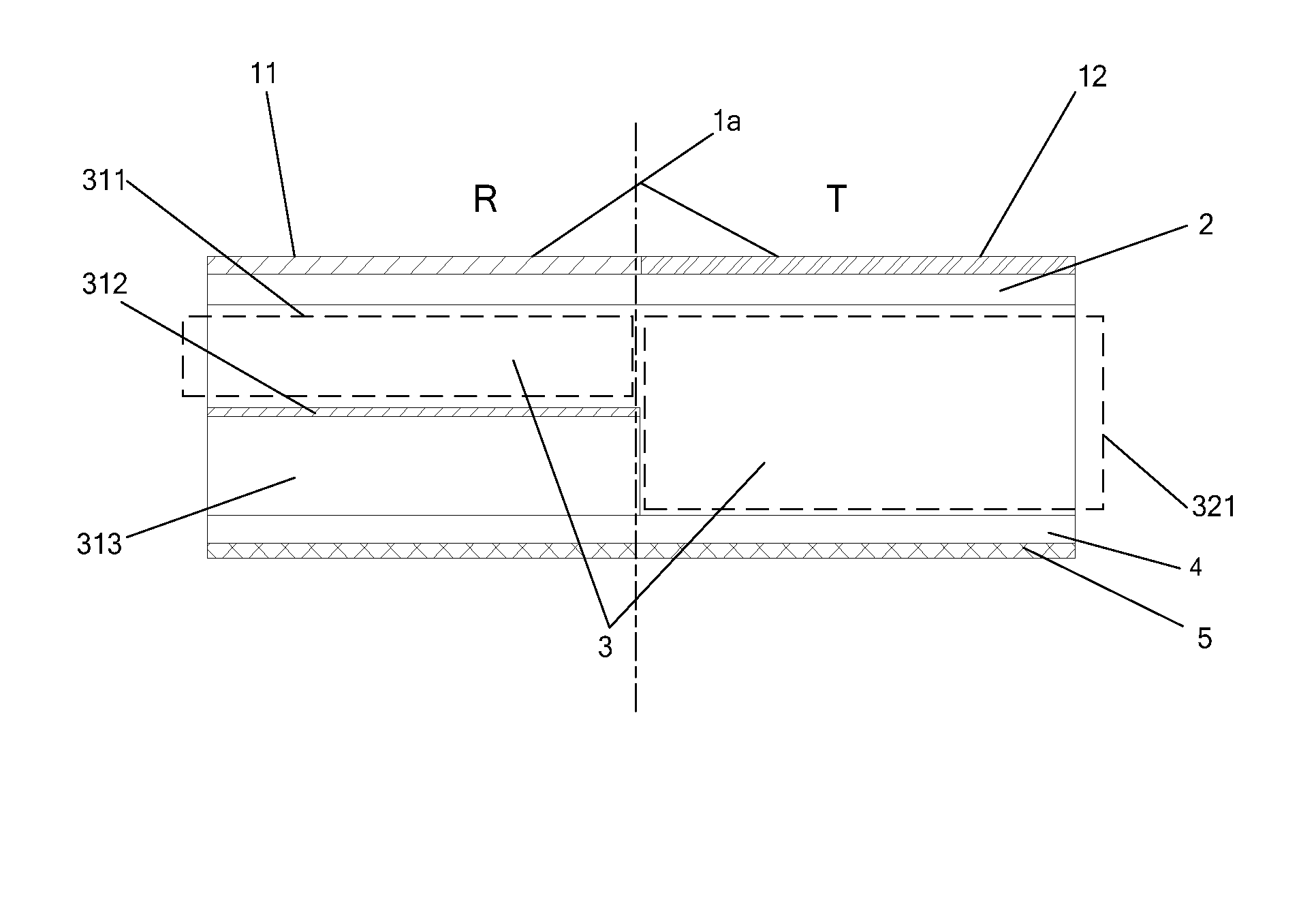
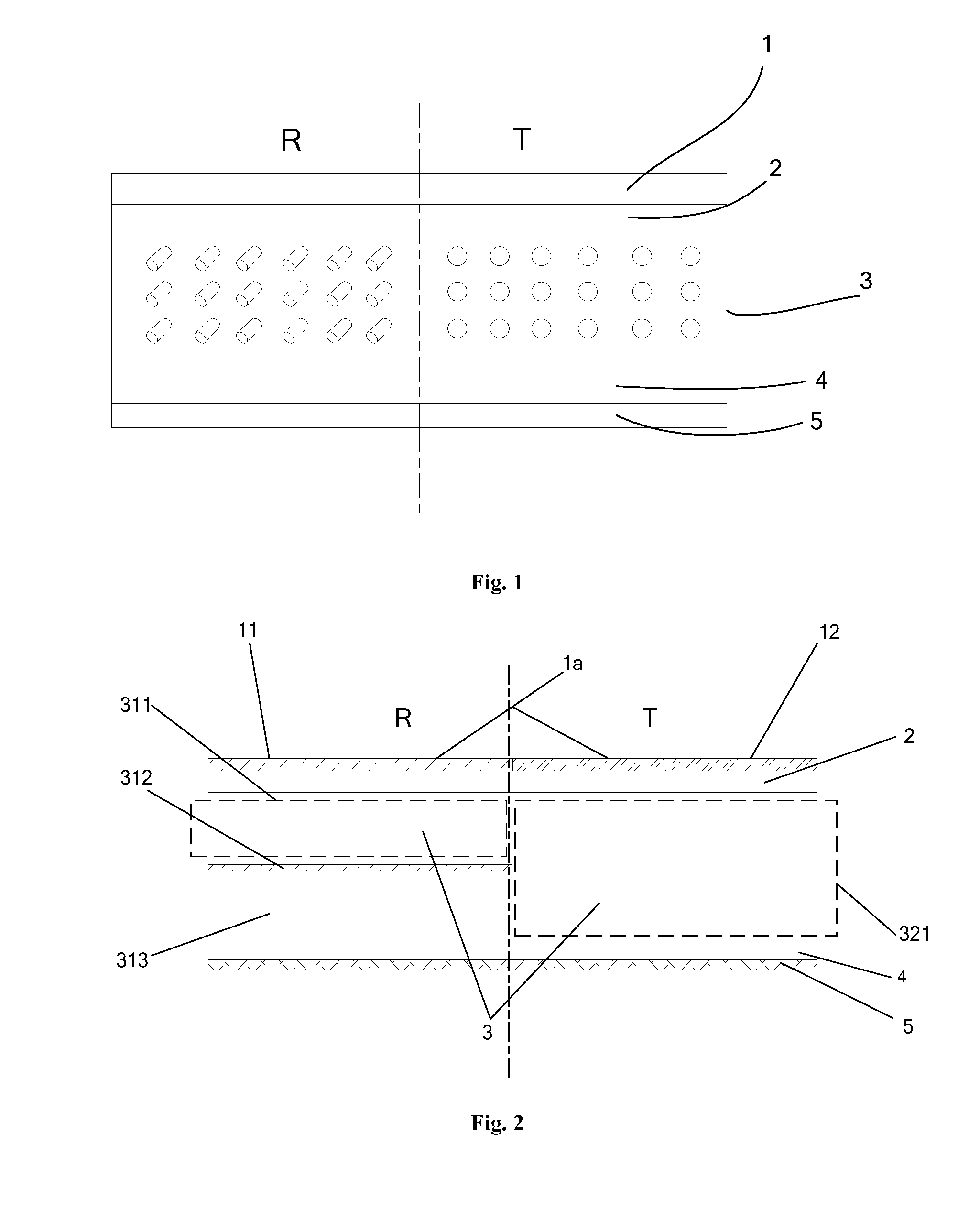
[0025]As shown in FIG. 2, the embodiment provides an ADS type transflective liquid crystal display panel, including a conductive polarizing film layer la, which is provided on an upper surface of an upper substrate 2 as an upper polarizing film layer of the liquid crystal display panel. The liquid crystal display panel further includes a lower substrate 4, and uniformly orientated liquid crystal layers 3 provided between the upper substrate 2 and the lower substrate 4. A lower polarizing layer 5 is provided on a lower surface of the lower substrate 4. A color filter (not shown) may be formed on the upper substrate 2, and a thin film transistor (not shown) may be formed below the lower substrate 4. Each pixel unit of the transflective liquid crystal display panel may include a transmission region T and a reflection region R. The liquid crystal l...


PUM

PropertyMeasurementUnit
thicknessaaaaaaaaaa
thicknessaaaaaaaaaa
conductiveaaaaaaaaaa

Abstract

The present invention discloses a transflective liquid crystal display panel and a liquid crystal display device comprising the same. Each pixel unit of the transflective liquid crystal display panel comprises a transmission region and a reflection region. The transflective liquid crystal display panel further comprises a conductive polarizing film layer having a first polarizing direction in the reflection region and a second polarizing direction in the transmission region.

Description

FIELD OF THE INVENTION[0001]The present invention relates to the field of liquid crystal display, and particularly relates to a transflective liquid crystal display panel and a display device.BACKGROUND OF THE INVENTION[0002]A typical transmissive display may have a reduced contrast of an image due to ambient light in outdoor environment or under bright light. By comparison, a reflective display, which relies on an external light source to achieve the display effect, exhibits better display effect and contrast in outdoor or under bright light, and can reduce a considerable amount of power consumed during use of backlight, thus the reflective display is very suitable for use in portable electronic products. However, when the brightness of the ambient light source is insufficient, the contrast and the brightness of the reflective display will be greatly influenced. Therefore, a transflective display, if manufactured by using a transmissive technique in combination with an auxiliary ba...

Claims


Application Information

Patent Timeline
Patent Type & Authority Applications(United States)
IPC IPC(8): G02F1/1335
CPCG02F1/133536G02F2001/133531G02F1/133555G02F1/133528G02F1/133538G02F1/133548G02F1/133531
Inventor KASHIMA, MIKI
Owner BOE TECH GRP CO LTD
Why Eureka
Try Eureka