Imprinted thin-film electronic sensor structure

a technology of electronic sensors and thin films, applied in the direction of dielectric characteristics, light absorption dielectrics, instruments, etc., can solve the problems of high cost of conventional integrated circuit techniques, high cost of photolithographic processes, and time-consuming laser ablation techniques, etc., to facilitate electrochemical detection, more sensitive electronic sensors, and greater electrode spatial resolution

Inactive Publication Date: 2016-02-18
EASTMAN KODAK CO
View PDF7 Cites 0 Cited by
  • Summary
  • Abstract
  • Description
  • Claims
  • Application Information

AI Technical Summary

Benefits of technology

[0050]The interdigitated microelectrode array is useful as an electrochemical sensor. A significant advantage of the present invention over the methods described in the prior art (e.g. laser ablation) is that the width and spacing of the microelectrode can be made very small, e.g. 2 to 10 microns, on a flexible substrate at reduced cost due to the simplicity of the manufacturing process and without sacrificing the quality of microelectrode dimension and spacing uniformity. Therefore the imprinted electronic sensor structure 5 provided by the present invention enables an accurate and precise readout from a relatively small analyte sample size, for example, less than 1 μL or less than 0.5 μL. In addition, the imprinted electronic sensor structure 5 as manufactured by a method of the present invention can have significantly improved diffusion recycling efficiency that enables highly sensitive electrochemical measurements with a high signal-to-noise ratio and a wide dynamic range.
[0051]The interdigitated microelectrode array can have a chemical coating deposited over the array to facilitate the practice of electrochemical detection. The chemical coating can contain a chemical reactive to produce an electro-active reaction product. Upon contacting the coating with a sample that contains an analyte, the analyte reacts with chemical compounds of the coating to generate an electro-active reaction product. This electro-active reaction product can be electronically detected, measured, or quantified by applying a potential difference between the electrodes and measuring the current at the working electrode.
[0052]In contrast to the thin-film electrical conductors of the present invention, thick-film conductors of the prior art, for example formed by processes such as screen printing silver paste, are not formed within the micro-channels 60 and are often limited in their width to widths that are directly visible to the unaided human visual system. Thus, the number of electrode sensors per linear area (as shown in FIG. 9, is smaller using such prior art methods than is enabled by embodiments of the present invention. An advantage of the present invention, therefore, is a greater electrode spatial resolution and a more sensitive electronic sensor at a lower cost.
[0053]In yet another embodiment, the imprinted electronic sensor structure 5 further includes an optical sensor 82 for sensing the optical state of the multi-layer micro-wires 50. In an embodiment, the optical state is combined with electrical signals derived by the controller 80 from the multi-layer micro-wires 50 to provide further information about the environmental factor 40. In an embodiment, the environmental factor 40 includes multiple environmental materials.
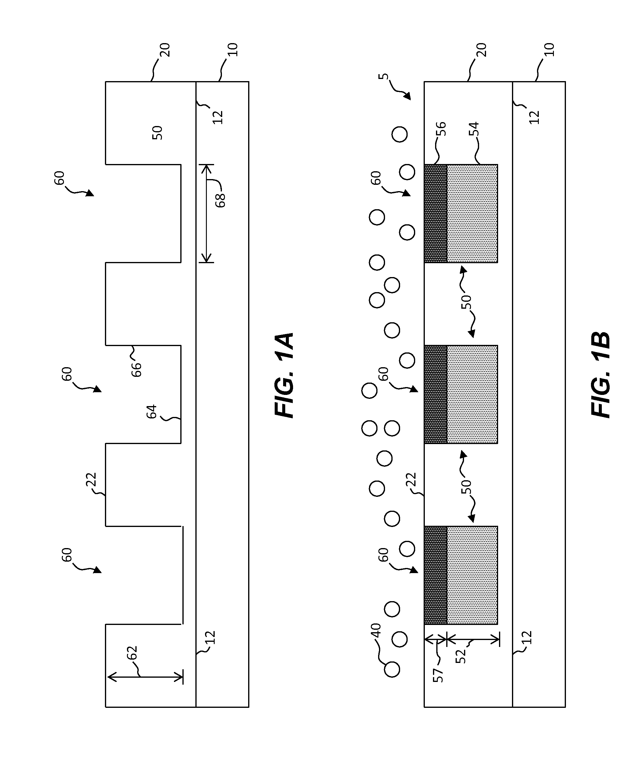
[0054]Referring to the successive cross sections of FIGS. 10-18 and the corresponding flow diagrams of FIGS. 21 and 23, a method according to the present invention of making the imprinted electronic sensor structure 5 includes providing the substrate 10 having the substrate surface 12 (FIG. 10) in step 100. Micro-channels 60 are then provided in step 110 by coating a curable layer 24 having the layer surface 22 on the substrate surface 12 of the substrate 10 in step 200 (FIGS. 11 and 23), imprinting the curable layer 24 in step 210, and curing the curable layer 24 in step 220 to form the cured layer 20 with a plurality of spatially separated imprinted micro-channels 60 on the substrate 10 (FIG. 12) extending from the layer surface 22 into the cured layer 20. Methods and materials for coating a single curable layer, imprinting the curable layer, and curing the curable layer are known in the art.
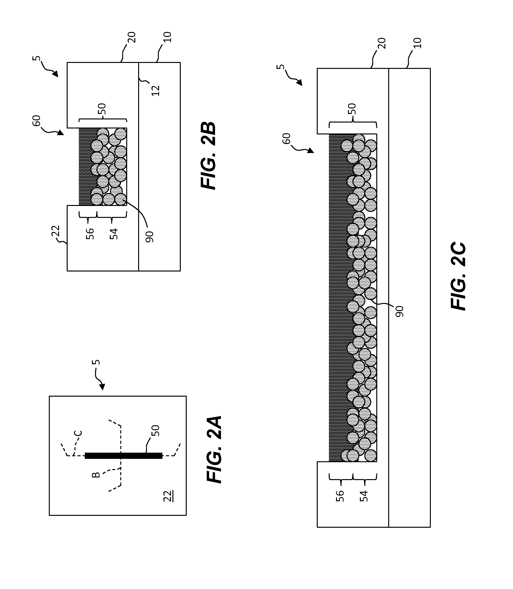
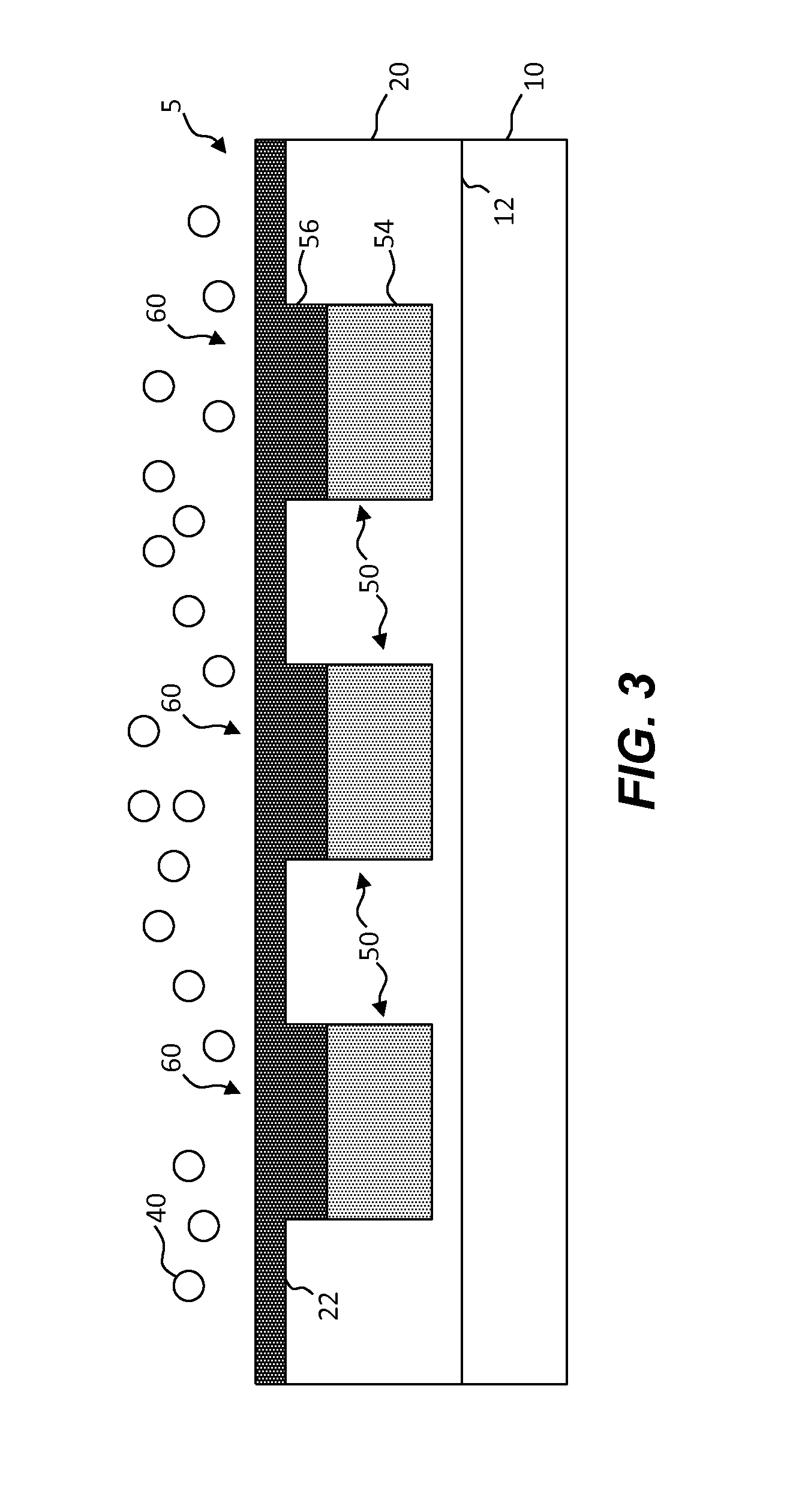
[0055]Referring next to FIGS. 13 and 21, a conductive material, in this case a curable conductive ink 30 is coated on the layer surface 22 of the cured layer 20 on the substrate 10 and in the micro-channels 60 in step 120. The curable conductive ink 30 is removed from the layer surface 22 of the cured layer 20 on the substrate 10 in step 130 (FIG. 14) leaving the curable conductive ink 30 in the micro-channels 60. Referring to FIG. 15, ultra-violet radiation 70 (or heat) cures the curable conductive ink 30 (FIG. 14) to form cured conductive ink 32 in the micro-channels 60 in the cured layer 20 on the substrate 10 in step 140. In this embodiment, the cured conductive ink 32 forms the conductive layer 54. In step 150, referring to FIG. 16, the conductive layer 54 in the micro-channels 60 and the layer surface 22 of the cured layer 20 on substrate 10 are coated (step 150) with a curable reactive material 55. In an optional step 160 similar to step 130, the curable reactive material 55 is removed from the layer surface 22 of the cured layer 20 on the substrate 10 (FIG. 17). As shown in FIG. 18, the curable reactive material 55 is cured in step 170 to form the cured reactive layer 56 with ultra-violet radiation 70 (or heat) to form the multi-layer micro-wires 50 in the cured layer 20 on the substrate 10. If the optional step 160 of removing, the curable reactive material 55 from the layer surface 22 is omitted, the structure illustrated in FIG. 3 is obtained.

Problems solved by technology

Such an electronic sensor is sometimes called an “electronic nose” and is typically fabricated on a silicon substrate using conventional integrated circuit techniques at a relatively high cost.
Photolithographic processes are known to be expensive, and generally require a rigid substrate for the formation of small feature size, e.g. <5 microns.
Laser ablation requires a time-consuming rastering technique if a complex electrode pattern is to be formed on the surface.
Moreover, the precision of the electrode edge is not well defined.
Although electronic sensors are widely useful, the cost associated with the desired feature sizes can limit their applicability.

Method used


Image

  • Imprinted thin-film electronic sensor structure
  • Imprinted thin-film electronic sensor structure
  • Imprinted thin-film electronic sensor structure

Examples


Embodiment Construction

[0030]The present invention provides an imprinted electronic sensor structure on a substrate for sensing an environmental factor. The imprinted electronic sensor structure includes a thin-film multi-layer micro-wire structure on a substrate that senses an environmental factor. In an embodiment, the thin-film multi-layer micro-wire structure is miniaturized with improved sensitivity, selectivity, and response time at reduced manufacturing costs.

[0031]Referring to FIGS. 1A and 1B, an imprinted electronic sensor structure 5 for sensing an environmental factor according to an embodiment of the present invention includes a substrate 10. A cured layer 20 has a layer surface 22 located on a substrate surface 12 of the substrate 10. A plurality of spatially separated micro-channels 60 extend from the layer surface 22 into the cured layer 20. Referring specifically to FIG. 1A, the micro-channels 60 are illustrated together with a micro-channel bottom 64, a micro-channel side 66, and a micro-...


PUM

PropertyMeasurementUnit
depthaaaaaaaaaa
feature sizeaaaaaaaaaa

Abstract

An imprinted electronic sensor structure on a substrate for sensing an environmental factor includes a cured layer having a layer surface located on the substrate. Spatially separated micro-channels extend from the layer surface into the cured layer. A multi-layer micro-wire is formed in each micro-channel. Each multi-layer micro-wire includes at least a conductive layer and a reactive layer. The reactive layer is exposed to the environmental factor. The conductive layer is a cured electrical conductor located only within the micro-channel and at least a portion of the reactive layer responds to the environmental factor.

Description

CROSS REFERENCE TO RELATED APPLICATIONS[0001]Reference is made to commonly-assigned co-pending U.S. patent application Ser. No. ______ (Attorney Docket No. K001821) filed concurrently herewith, entitled “Making Imprinted Thin-film Electronic Sensor Structure”, by Lebens et al, to commonly-assigned co-pending U.S. patent application Ser. No. ______ (Attorney Docket No. K001822) filed concurrently herewith, entitled “Operating Imprinted Thin-film Electronic Sensor Structure”, by Lebens et al, and to commonly assigned U.S. patent application Ser. No. 13 / 779,917 filed Feb. 28, 2013, entitled “Multi-Layer Micro-Wire Structure” by Yau et al, the disclosures of which are incorporated herein.FIELD OF THE INVENTION[0002]The present invention relates to electronic sensors imprinted in a substrate.BACKGROUND OF THE INVENTION[0003]Electronic sensors for detecting and evaluating materials such as liquids and gases found in the environment are known. Such an electronic sensor is sometimes called ...

Claims


Application Information

Patent Timeline
Patent Type & Authority Applications(United States)
IPC IPC(8): G01N27/07G01N27/12
CPCG01N27/07G01N27/126G02F1/13439G06F2203/04103H05K3/0014H05K2201/0108H05K2201/0112H05K2201/0257H05K2201/0338H05K2201/2054H05K2203/1131H05K2203/1476H05K3/1258H05K2201/0269H05K2201/0272H05K2201/0376H05K2203/0108G06F3/0443
Inventor LEBENS, JOHN ANDREWCOK, RONALD STEVENWANG, YONGCAI
Owner EASTMAN KODAK CO
Why Eureka
Try Eureka