Integrated circuits with a bowed substrate, and methods for producing the same

Inactive Publication Date: 2016-03-03
GLOBALFOUNDRIES INC
View PDF4 Cites 3 Cited by
  • Summary
  • Abstract
  • Description
  • Claims
  • Application Information

AI Technical Summary

Benefits of technology

This patent describes methods for manufacturing integrated circuits with certain features. These features include the use of first and second STI insulators in a substrate, bowing of the substrate surface between the insulators, and the formation of a transistor between the insulators. The technical effect of these methods is the production of integrated circuits with improved performance and reliability. The patent also provides integrated circuits with the described features.

Problems solved by technology

However, decreasing the size of integrated circuits is a high priority, so simply producing wider FETs is not desirable.

Method used


Image

  • Integrated circuits with a bowed substrate, and methods for producing the same
  • Integrated circuits with a bowed substrate, and methods for producing the same
  • Integrated circuits with a bowed substrate, and methods for producing the same

Examples


Embodiment Construction

[0011]The following detailed description is merely exemplary in nature and is not intended to limit the various embodiments or the application and uses thereof. Furthermore, there is no intention to be bound by any theory presented in the preceding background or the following detailed description.

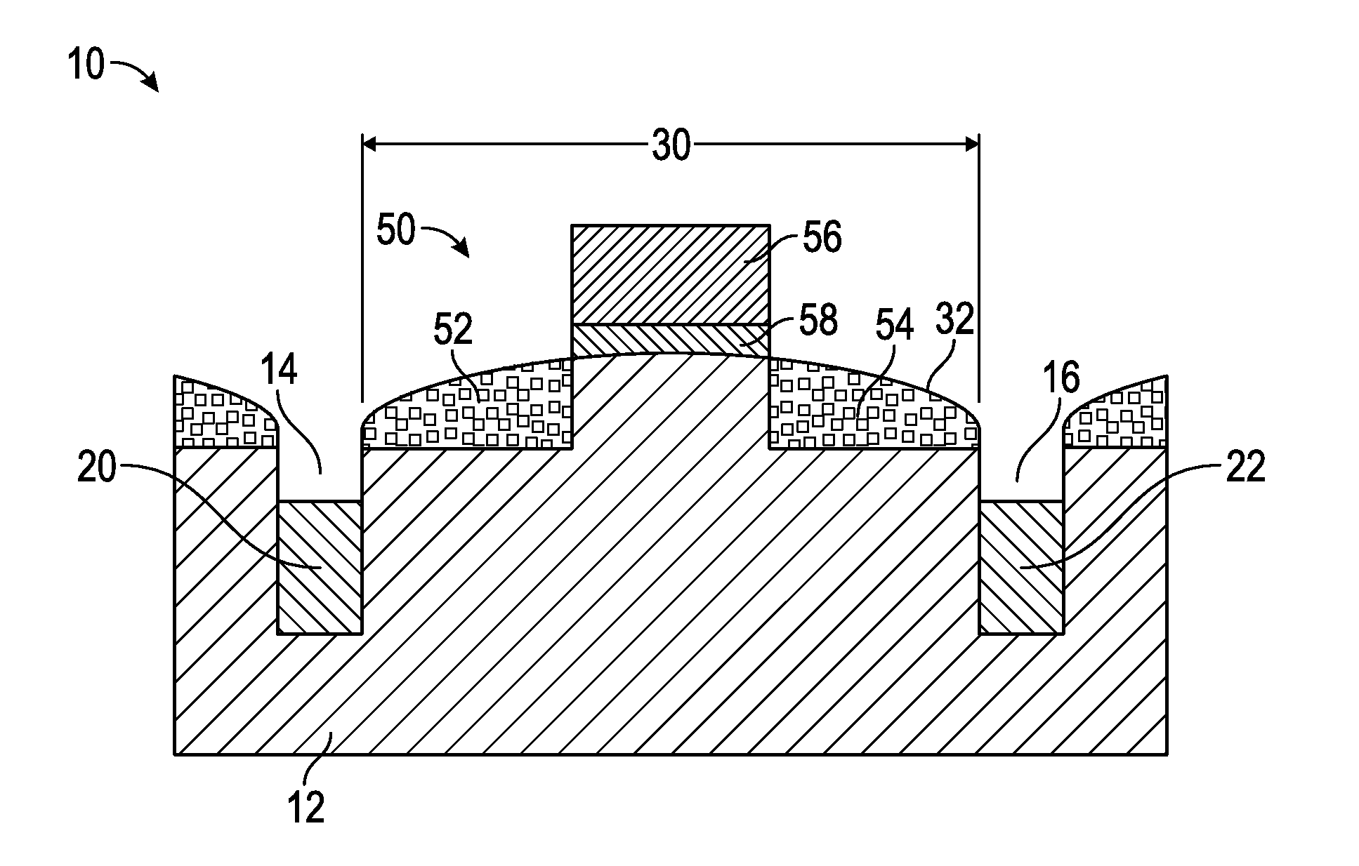
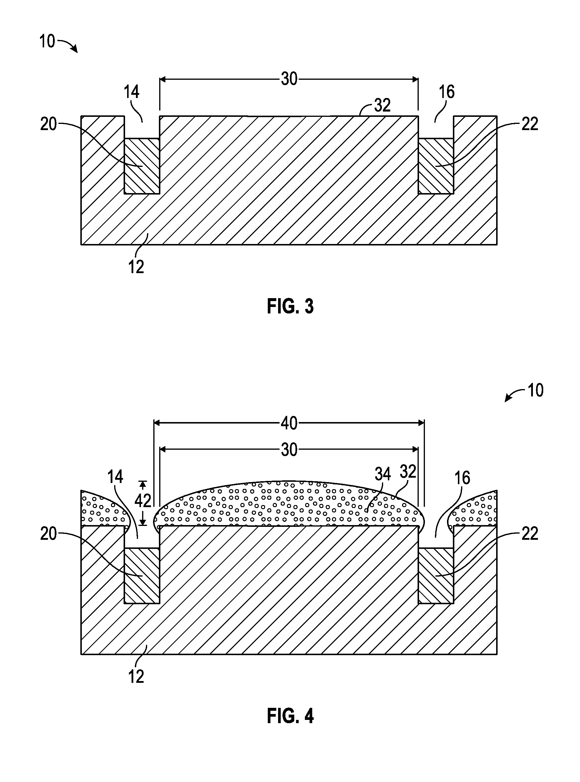
[0012]An integrated circuit begins with the production of first and second STI insulators, and the STI insulators are recessed to below a substrate surface. The substrate surface between the first and second STI insulators is then bowed. This increases the effective device width, because the distance between the STI insulators along a bowed surface is greater than the straight line distance between the STI insulators. The STI insulators are formed using standard techniques, so the variation in the distance between the STI insulators is consistent with traditional approaches. The substrate surface can be bowed using different techniques. For example, a cap formed by epitaxial growth can exte...


PUM


Abstract

Integrated circuits and methods for manufacturing the same are provided. A method for manufacturing an integrated circuit includes forming a first and second STI insulator in a substrate, and bowing a substrate surface between the first and second STI insulators. A transistor is formed between the first and second STI insulators.

Description

TECHNICAL FIELD[0001]The technical field generally relates to integrated circuits and methods for producing integrated circuits, and more particularly relates to integrated circuits with transistors overlying a bowed substrate and methods for producing the same.BACKGROUND[0002]The majority of present day integrated circuits (ICs) are implemented by using a plurality of interconnected field effect transistors (FETs), also called metal oxide semiconductor field effect transistors (MOSFETs or MOS transistors). A MOS transistor includes a gate electrode as a control electrode overlying a semiconductor substrate. Spaced-apart source and drain regions are on opposite sides of a channel in the substrate between which a current can flow. A gate insulator is disposed between the gate electrode and the channel to electrically isolate the gate electrode from the substrate. A control voltage applied to the gate electrode controls the flow of current through the channel in the substrate underlyi...

Claims


Application Information

Patent Timeline
IPC IPC(8): H01L21/324H01L29/66H01L21/762H01L29/06H01L29/78
CPCH01L29/66477H01L21/76224H01L29/0653H01L29/78H01L29/0657H01L21/3247H01L21/2636H01L29/66651H01L29/1037H01L29/1054H01L29/165H01L21/02532H01L21/0262
Inventor RICHTER, RALFZSCHATZSCH, GERDWASYLUK, JOANNA
Owner GLOBALFOUNDRIES INC
Why Eureka
Try Eureka