Multi-fin multi-gate field effect transistor with tailored drive current

a field effect transistor and drive current technology, applied in the field of multi-fin multi-gate field effect transistors, can solve the problems of increased power, reduced performance, and significant quantization, and achieve the effect of increasing the drive current of the device, and reducing the number of transistors

Active Publication Date: 2009-08-20
GLOBALFOUNDRIES US INC
View PDF6 Cites 33 Cited by
  • Summary
  • Abstract
  • Description
  • Claims
  • Application Information

AI Technical Summary

Benefits of technology

[0010]In view of the foregoing disclosed herein are embodiments of an improved multi-gated field effect transistor (MUGFET) structure and method of forming the MUGFET structure so that it exhibits a more tailored drive current. Specifically, the MUGFET incorporates multiple semiconductor fins in order to increase effective channel width of the device and, thereby, to increase the drive current of the device. Additionally, the MUGFET incorporates a gate structure having different sections with different physical dimensions relative to the semiconductor fins in order to more finely tune device drive current (i.e., to achieve a specific drive current). Optionally, the MUGFET also incorporates semiconductor fins with differing widths in order to minimize leakage current caused by increases in drive current.

Problems solved by technology

However, for multi-fin MUGFETs quantization is a significant issue.
That is, if device drive is not optimized, quantization can result in additional power and lower performance.
However, tradeoffs are associated with each of these alternatives and these tradeoffs typically include additional processing which adds to the wafer cost and development complexity.
For example, reducing the physical dimensions of the second section of the gate relative to each second semiconductor fin, as compared to the physical dimensions of the first section relative to each first semiconductor fin, can result in an increase in device drive current.
Contrarily, increasing the physical dimensions of the second section of the gate relative to each second semiconductor fin as compared to the physical dimensions of the first section relative to each first semiconductor fin can result in a decrease in device drive current.
That is, an increase in drive current will typically result in a corresponding increase in leakage current.
For example, reducing the physical dimensions of the second section of the gate relative to each second semiconductor fin as compared to the physical dimensions of the first section relative to each first semiconductor fin can result in an increase in device drive current.
Contrarily, increasing the physical dimensions of the second section of the gate relative to each second semiconductor fin as compared to the physical dimensions of the first section relative to each first semiconductor fin can result in a decrease in device drive current.
That is, an increase in drive current will typically result in a corresponding increase in leakage current.

Method used


Image

  • Multi-fin multi-gate field effect transistor with tailored drive current
  • Multi-fin multi-gate field effect transistor with tailored drive current
  • Multi-fin multi-gate field effect transistor with tailored drive current

Examples


Embodiment Construction

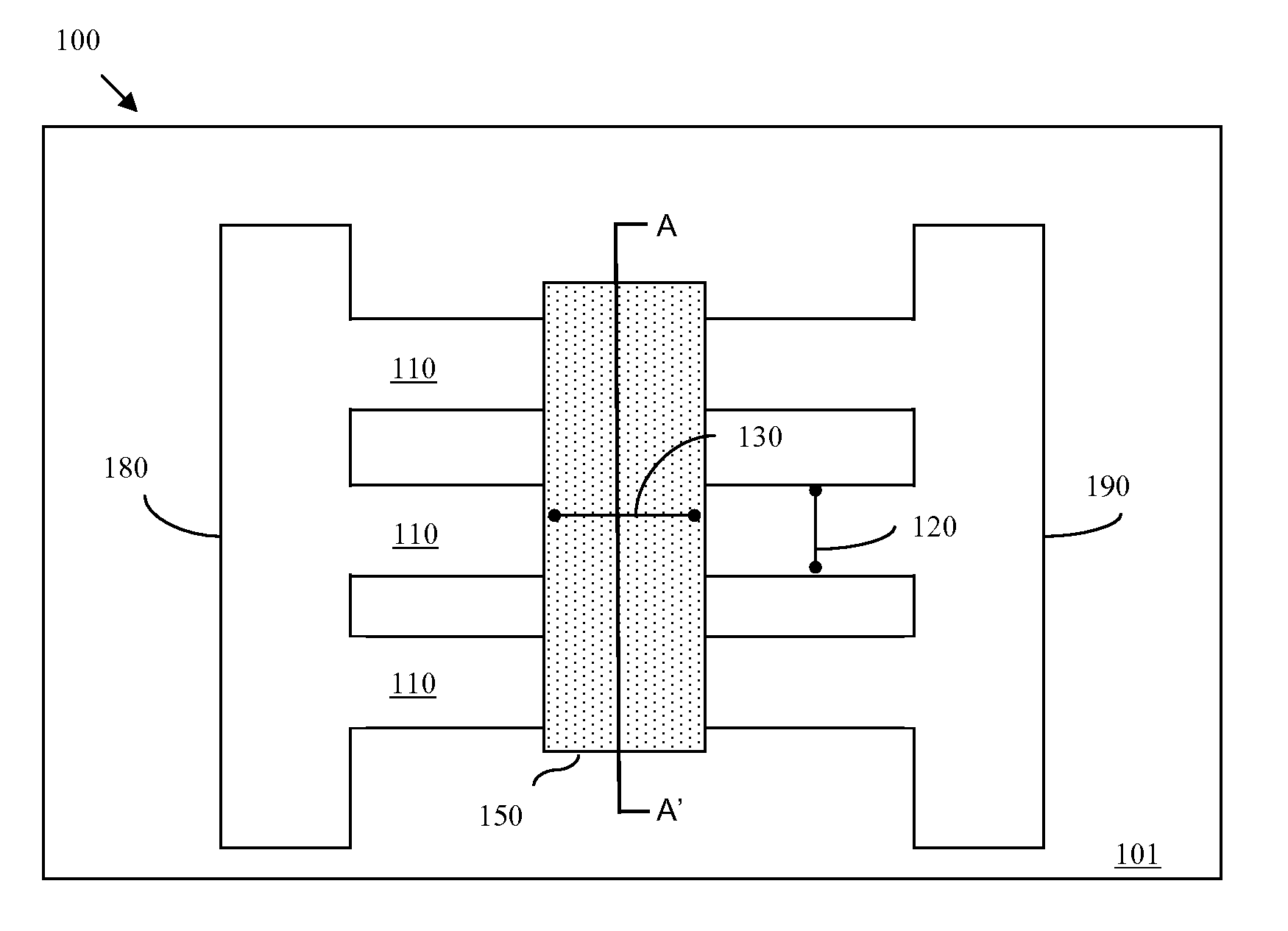
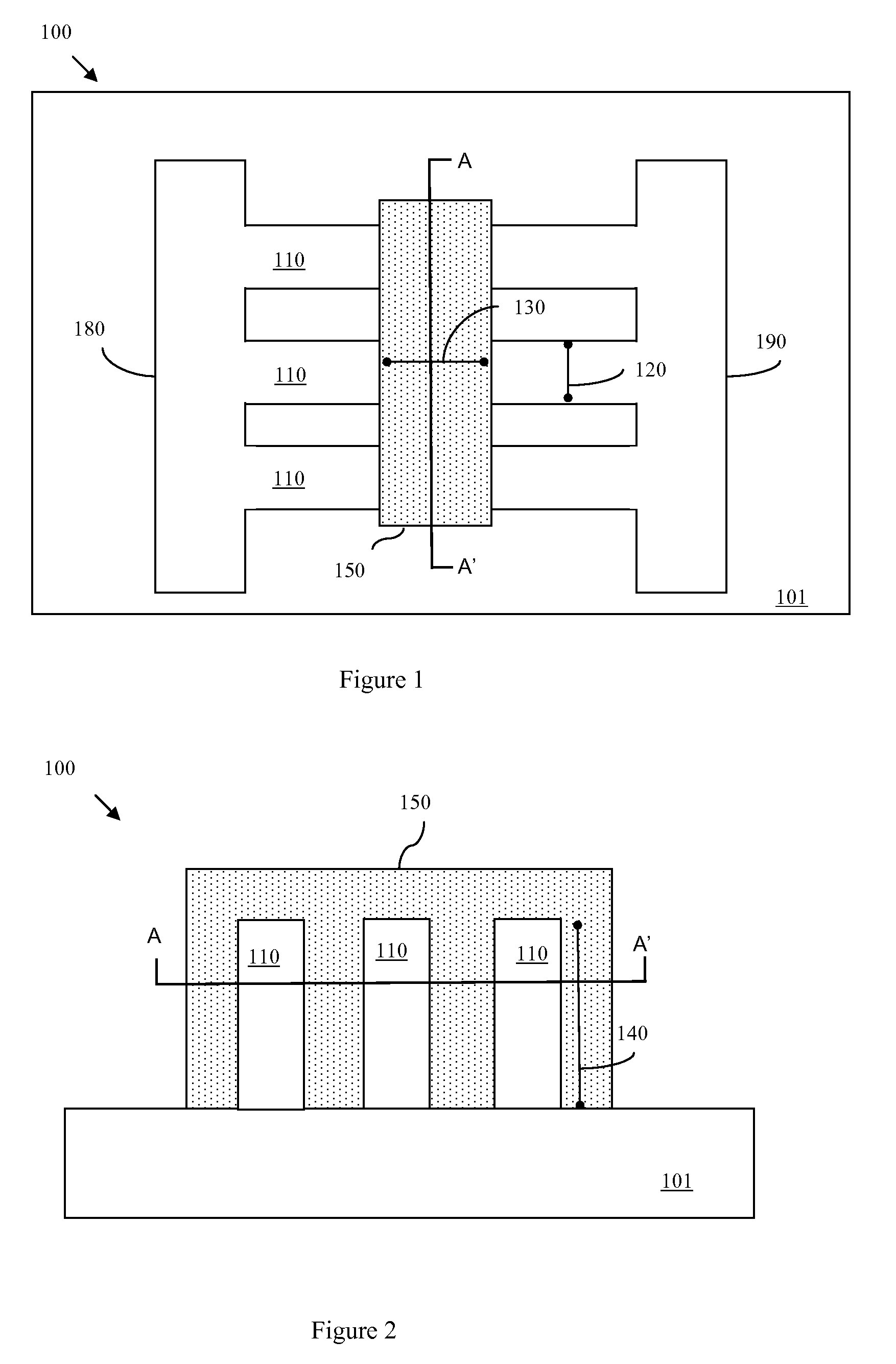
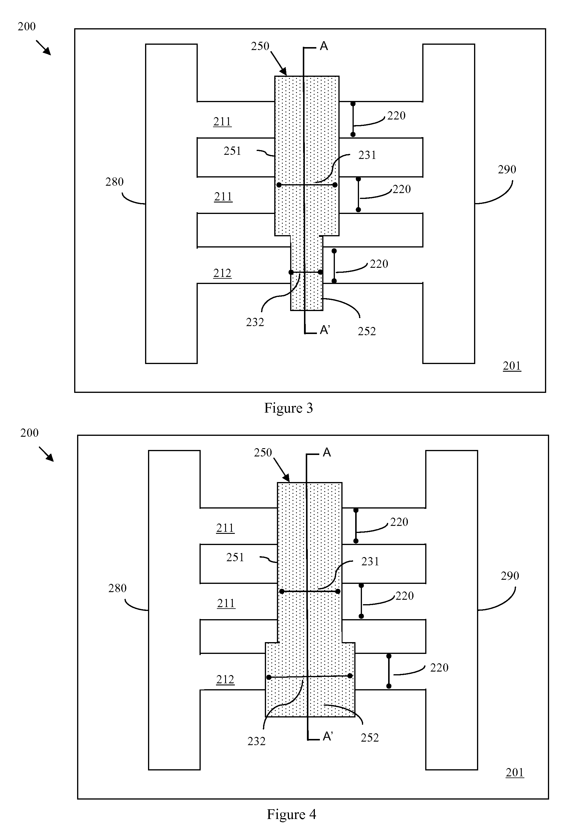
[0050]The embodiments of the invention and the various features and advantageous details thereof are explained more fully with reference to the non-limiting embodiments that are illustrated in the accompanying drawings and detailed in the following description. It should be noted that the features illustrated in the drawings are not necessarily drawn to scale. Descriptions of well-known components and processing techniques are omitted so as to not unnecessarily obscure the embodiments of the invention. The examples used herein are intended merely to facilitate an understanding of ways in which the embodiments of the invention may be practiced and to further enable those of skill in the art to practice the embodiments of the invention. Accordingly, the examples should not be construed as limiting the scope of the embodiments of the invention.

[0051]As discussed above, multi-gated non-planar field effect transistors (MUGFETs), such as fin-type FETs (finFETs)) or trigate FETs, were deve...


PUM


Abstract

Disclosed are embodiments of an improved multi-gated field effect transistor (MUGFET) structure and method of forming the MUGFET structure so that it exhibits a more tailored drive current. Specifically, the MUGFET incorporates multiple semiconductor fins in order to increase effective channel width of the device and, thereby, to increase the drive current of the device. Additionally, the MUGFET incorporates a gate structure having different sections with different physical dimensions relative to the semiconductor fins in order to more finely tune device drive current (i.e., to achieve a specific drive current). Optionally, the MUGFET also incorporates semiconductor fins with differing widths in order to minimize leakage current caused by increases in drive current.

Description

CROSS-REFERENCE TO RELATED APPLICATIONS[0001]This application is related to the following co-pending application filed concurrently herewith by the same Applicants and assigned to the same Assignee: “A METHOD OF FORMING A MULTI-FIN MULTI-GATE FIELD EFFECT TRANSISTOR WITH TAILORED DRIVE CURRENT”, Attorney Docket No. BUR920070094US2. The complete disclosure of this co-pending application is incorporated herein by reference.BACKGROUND[0002]1. Field of the Invention[0003]The embodiments of the invention generally relate to multi-fin, multi-gated field effect transistors (MUGFETS), and, more particularly, a multi-fin MUGFET structure and method in which drive current is tailored by varying the physical dimensions of the gate over one or more of the semiconductor fins.[0004]This application is related to the following co-pending application filed concurrently herewith by the same Applicants and assigned to the same Assignee: “A METHOD OF FORMING A MULTI-FIN MULTI-GATE FIELD EFFECT TRANSIS...

Claims


Application Information

Patent Timeline
Patent Type & Authority Applications(United States)
IPC IPC(8): H01L29/78
CPCH01L29/785H01L29/66795
Inventor ANDERSON, BRENT A.NOWAK, EDWARD J.
Owner GLOBALFOUNDRIES US INC
Why Eureka
Try Eureka