Static random access memory and method thereof

a random access memory and random access technology, applied in static storage, information storage, digital storage, etc., can solve the problems of low mos capacitance value in low-voltage operation, inability to read disturb voltage undesired, and inability to read disturb voltage, etc., to improve writability, improve writability, and improve write margin

Active Publication Date: 2016-04-14
M31 TECH
View PDF0 Cites 0 Cited by
  • Summary
  • Abstract
  • Description
  • Claims
  • Application Information

AI Technical Summary

Benefits of technology

[0009]In view of the foregoing, it is an object of the embodiment of the present invention to provide a SRAM with an enhanced write margin and / or a lower Vmin. In one embodiment, the SRAM provides a negative bit line voltage to improve writability, and furnishes power supply voltage drop to assist in discharging at a bit node.

Problems solved by technology

Conventional SRAM suffers from half-select disturb phenomenon as a word line may simultaneously turn on the SRAM cells adjacent to the selected one of the same row, causing the adjacent SRAM cells to unwanted discharge.
Moreover, as the SRAM cell is selected and read, a read disturb voltage may be undesirably rendered due to voltage divider made of an access transistor and a pull-down transistor.
The word line boosting scheme, however, suffers from low MOS capacitance value in a low-voltage operation, limited cells number associated with a word line, and half-select disturb.

Method used


Image

  • Static random access memory and method thereof
  • Static random access memory and method thereof
  • Static random access memory and method thereof

Examples


Embodiment Construction

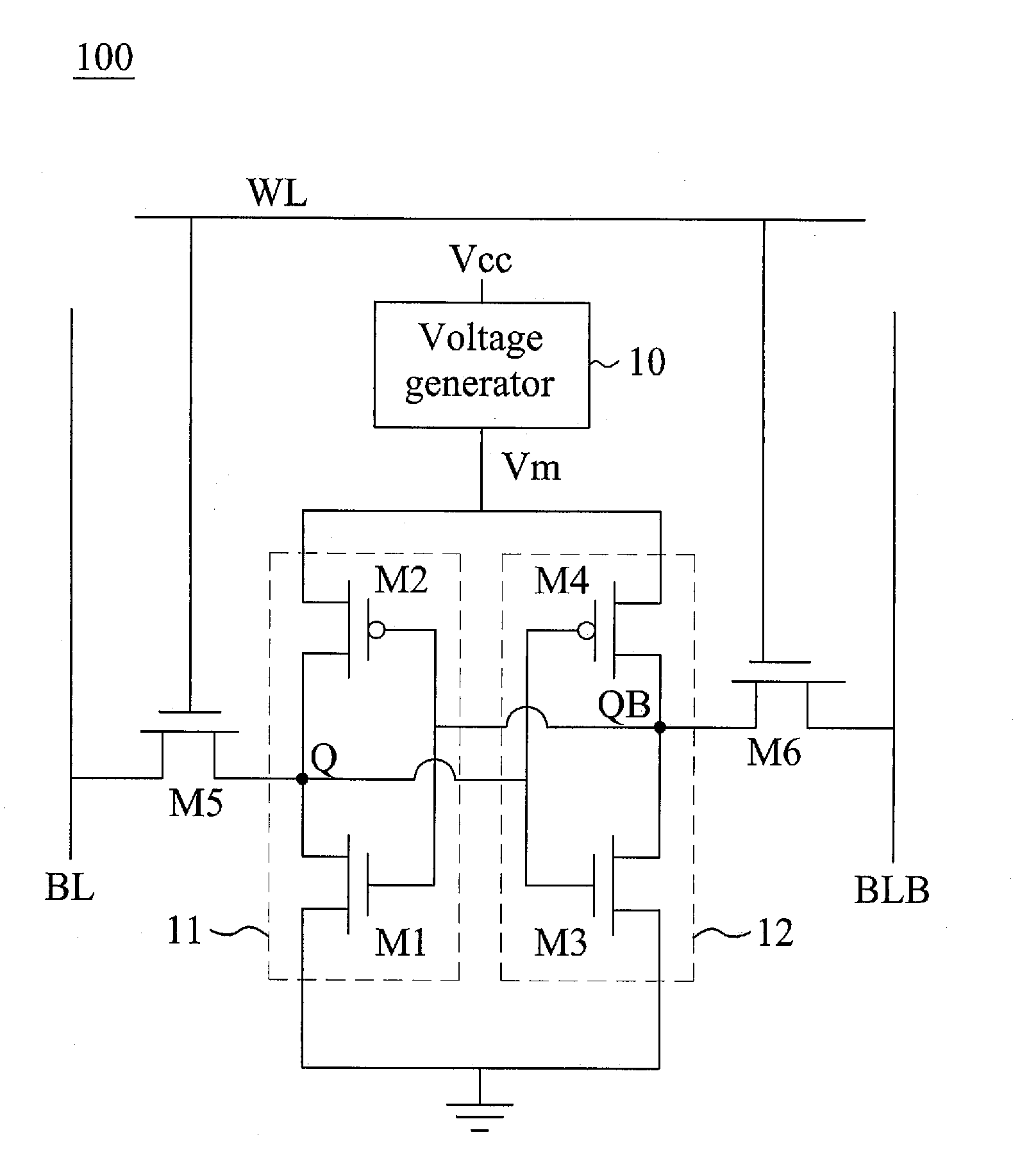
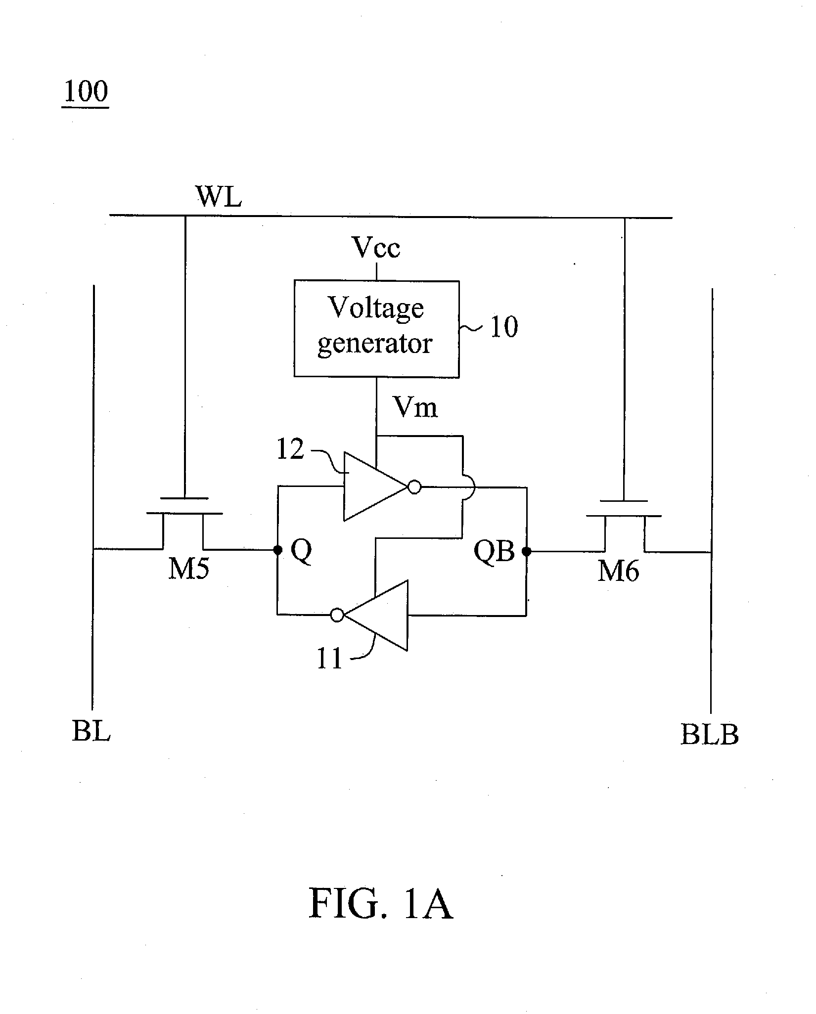
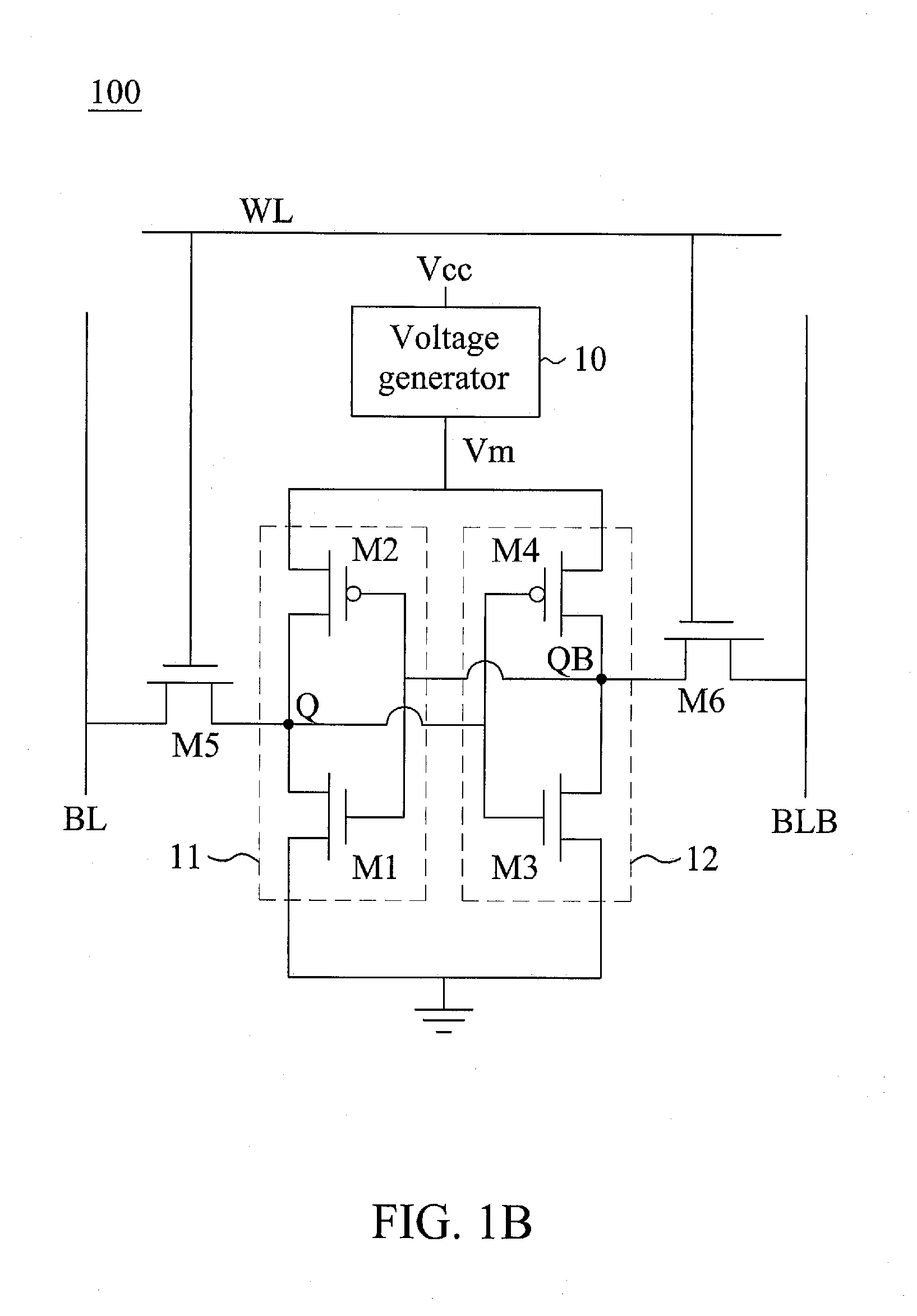
[0018]FIG. 1A shows a circuit diagram illustrated of a static random access memory (SRAM) 100 according to one embodiment of the present invention, and FIG. 1B shows a detailed circuit diagram of the SRAM 100 of FIG. 1A. One SRAM cell is representatively shown, and a plurality of the same SRAM cells may be arranged in an array of rows and columns to form a SRAM device. Although a 6-T SRAM is illustrated in the following embodiment, it is appreciated that the present invention may be embodied in other SRAM with different number of transistor, or may be embodied in a dual-port SRAM.

[0019]The SRAM 100 of the embodiment includes a voltage generator 10 that is coupled to receive a positive power supply voltage Vcc, and is configured to controllably generate a first power supply voltage Vm, wherein the first power supply voltage is with a reduced level and is higher than a retention voltage during a specific period. The positive power supply voltage Vcc of the embodiment may be as low as ...


PUM


Abstract

A static random access memory (SRAM) includes a voltage generator coupled to receive a positive power supply voltage, and to controllably generate a first power supply voltage, which is with a reduced level and is higher than a retention voltage during a specific period. A first inverter and a second inverter each is connected between the first power supply voltage and a second power supply voltage. The first inverter and the second inverter are cross-coupled, and the output nodes of the first inverter and the second inverter act as a bit node pair.

Description

BACKGROUND OF THE INVENTION[0001]1. Field of the Invention[0002]The present invention generally relates to a static random access memory (SRAM), and more particularly to a SRAM having an enhanced write margin with scaled power supply voltage.[0003]2. Description of Related Art[0004]Static random access memory (SRAM) is a type of semiconductor memory device that uses a latch to store a bit of information without a need of periodical refreshing as required in a dynamic random access memory (DRAM). A typical SRAM cell is made up of six transistors (6-T), while more transistors (e.g., 8-T) or fewer transistors (e.g., 4-T) may be available. SRAM cells are ordinarily arranged in an array of rows and columns. A word line is connected to, and is used to select, SRAM cells of the associated row. A pair of bit lines is connected to SRAM cells of the associated column, through which the SRAM cell may be read out or written into a bit of information.[0005]As integrated circuits have been scaled...

Claims


Application Information

Patent Timeline
Patent Type & Authority Applications(United States)
IPC IPC(8): G11C11/419
CPCG11C11/419G11C11/417G11C7/1051G11C7/22G11C7/1078
Inventor LIEN, NAN-CHUN
Owner M31 TECH
Why Eureka
Try Eureka