
Vertical high-voltage mos transistor and method of forming the mos transistor with improved on-state resistance

a technology of vertical high-voltage mos transistor and on-state resistance, which is applied in the direction of transistors, electrical devices, semiconductor devices, etc., can solve the problems of significant silicon real estate consumption of high-voltage mos transistors, and achieve the effect of improving on-state resistan

Active Publication Date: 2016-06-09
TEXAS INSTR INC
View PDF6 Cites 12 Cited by
  • Summary
  • Abstract
  • Description
  • Claims
  • Application Information

AI Technical Summary

Benefits of technology

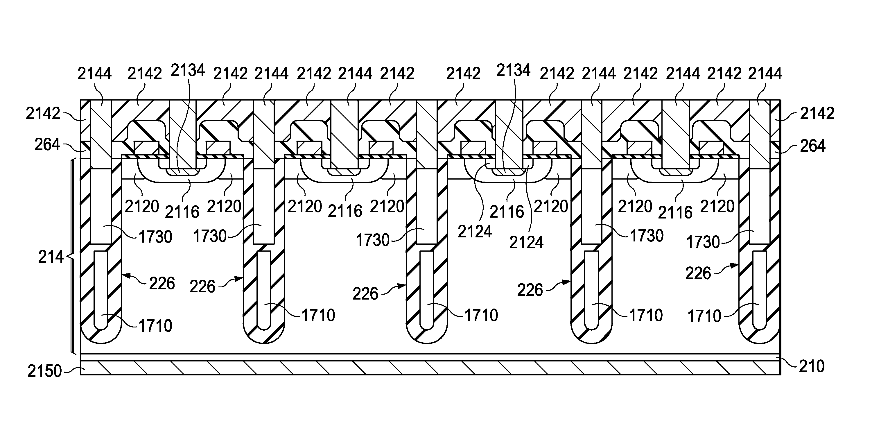
The present invention is a vertical high-voltage MOS transistor that improves on-state resistance. It includes a semiconductor material with trench structures and body regions with a second conductivity type. The transistor also has LDD regions and source and drain regions with the first conductivity type. The invention provides improved performance by improving the ON-state resistance, the current-carrying capacity, and the stability of the transistor.

Problems solved by technology

When formed to be structurally similar to a low-voltage MOS transistor, a high-voltage MOS transistor consumes a significant amount of silicon real estate due to the space required by the relatively large drain drift region.

Method used


Image

  • Vertical high-voltage mos transistor and method of forming the mos transistor with improved on-state resistance
  • Vertical high-voltage mos transistor and method of forming the mos transistor with improved on-state resistance
  • Vertical high-voltage mos transistor and method of forming the mos transistor with improved on-state resistance

Examples


Embodiment Construction

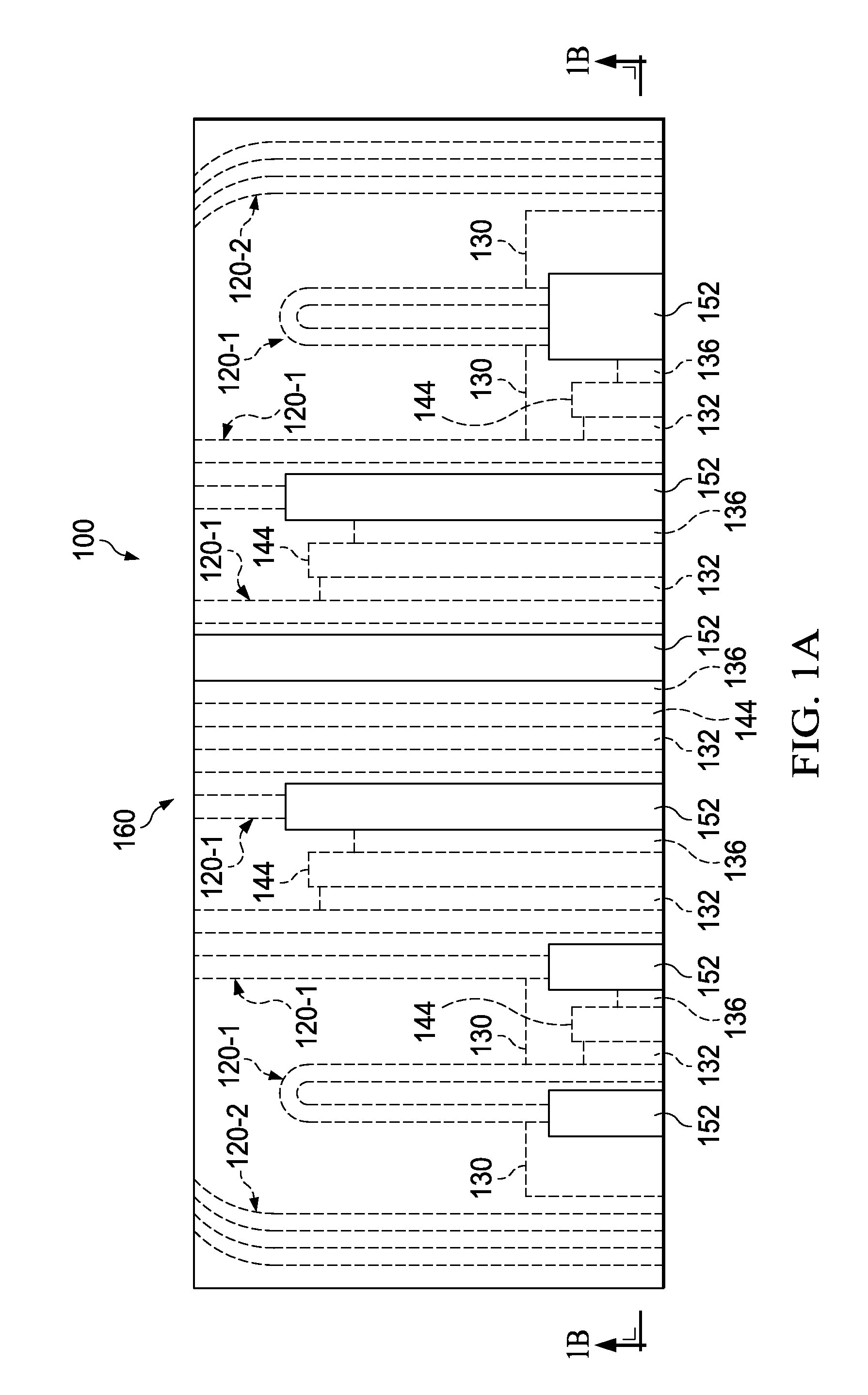
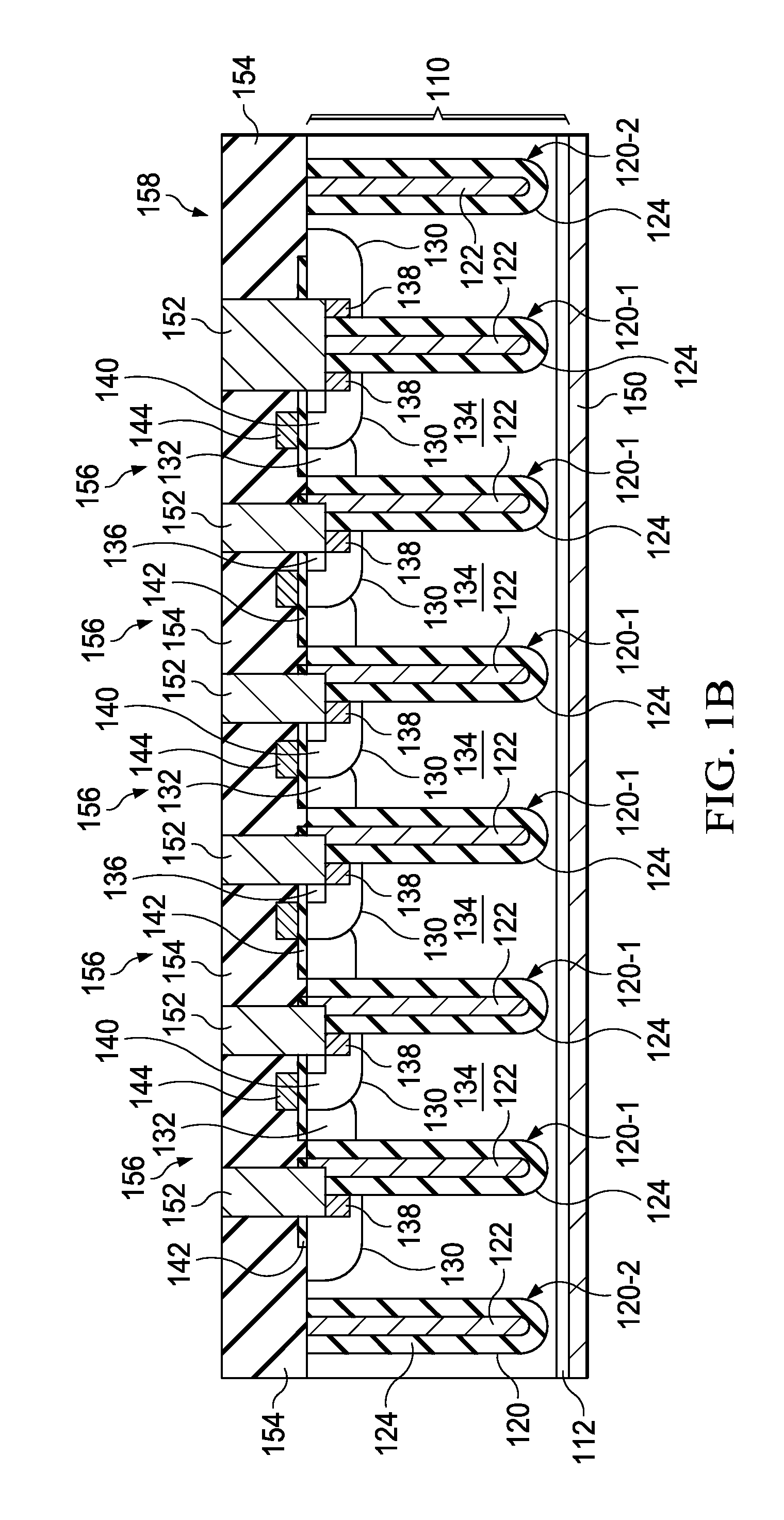
[0020]FIGS. 1A-1B show views that illustrate an example of a vertical high-voltage MOS transistor 100 in accordance with the present invention. FIG. 1A shows a partial plan view, while FIG. 1B shows a cross-sectional view taken along lines 1B-1B of FIG. 1A. As described in greater detail below, MOS transistor 100, which includes a number of trenches, increases the on-state resistance by reducing the trench pitch, which is the distance from a point on a trench to a corresponding point on an adjacent trench.

[0021]As shown in FIGS. 1A-1B, MOS transistor 100 includes a semiconductor region 110 and a drain region 112 that is formed to extend from the bottom surface of semiconductor region 110 up a distance into semiconductor region 110. In the present example, semiconductor region 110 and drain region 112 both have an n conductivity type, while drain region 112 has a much higher dopant concentration, being formed to be heavily doped.

[0022]As further shown in FIGS. 1A-1B, MOS transistor 1...


PUM


Abstract

A vertical, high-voltage MOS transistor, which has a source region, a body contact region, and a number of trenches structures with field plates, and a method of forming the MOS transistor increase the on-state resistance of the MOS transistor by reducing the trench pitch. Trench pitch can be reduced with metal contacts that simultaneously touch the source regions, the body contact regions, and the field plates. Trench pitch can also be reduced with a gate that increases the size of the LDD region.

Description

BACKGROUND OF THE INVENTION[0001]1. Field of the Invention[0002]The present invention relates to high-voltage MOS transistors and, more particularly, to a vertical high-voltage MOS transistor and a method of forming the MOS transistor with improved on-state resistance.[0003]2. Description of the Related Art[0004]A metal oxide semiconductor (MOS) transistor is a well-known semiconductor device that has a source, a drain, a body that has a channel region that lies between and touches the source and drain, and a gate that lies over and is isolated from the channel region by a gate dielectric layer. There are two types of MOS transistors: an NMOS transistor that has n+ source and drain regions with a p-type channel region, and a PMOS transistor that has p+ source and drain regions with an n-type channel region.[0005]In operation, when the source and the body are grounded, a positive voltage is placed on the drain to set up a drain-to-source electric field, and a voltage is placed on the...

Claims


Application Information

Patent Timeline
Patent Type & Authority Applications(United States)
IPC IPC(8): H01L29/40H01L29/06H01L29/417H01L29/66H01L29/78H01L29/08
CPCH01L29/404H01L29/407H01L29/7802H01L29/7827H01L29/0882H01L29/0865H01L29/7835H01L29/0878H01L29/41741H01L29/66666H01L29/66712H01L29/0696H01L29/086H01L29/41766H01L29/66727H01L29/7811H01L21/763H01L29/1095H01L29/66348H01L29/7803H01L29/783H01L29/7832
Inventor KOCON, CHRISTOPHER BOGUSLAWMOLLOY, SIMON JOHNNEILSON, JOHN MANNING SAVIDGEKAWAHARA, HIDEAKI
Owner TEXAS INSTR INC
Learn More