Manufacturing method of an HEMT transistor of the normally off type with reduced resistance in the on state and HEMT transistor

Active Publication Date: 2019-07-25
STMICROELECTRONICS SRL
View PDF2 Cites 2 Cited by
  • Summary
  • Abstract
  • Description
  • Claims
  • Application Information

AI Technical Summary

Benefits of technology

The present invention provides a transistor that has a high threshold voltage and low ON state resistance. This solution helps to overcome the problems that were previously present in the prior art.

Problems solved by technology

A known drawback of the HEMT 1, and in general of p-GaN gate transistors, is due to their relatively low threshold voltage.
However, increasing the concentration of doping in the doped gate region 12 leads indirectly to an undesired increase in the ON state resistance (RON) of the HEMT device 1.
The presence of magnesium in said regions of the heterostructure 7 leads to a partial depletion of the 2DEG and consequently an undesired increase in the ON state resistance.
Further, the chemical etching carried out in the third step may lead to an undesired reduction in the thickness of the barrier layer 9, and consequently a further increase in the ON state resistance.

Method used


Image

  • Manufacturing method of an HEMT transistor of the normally off type with reduced resistance in the on state and HEMT transistor
  • Manufacturing method of an HEMT transistor of the normally off type with reduced resistance in the on state and HEMT transistor
  • Manufacturing method of an HEMT transistor of the normally off type with reduced resistance in the on state and HEMT transistor

Examples


Embodiment Construction

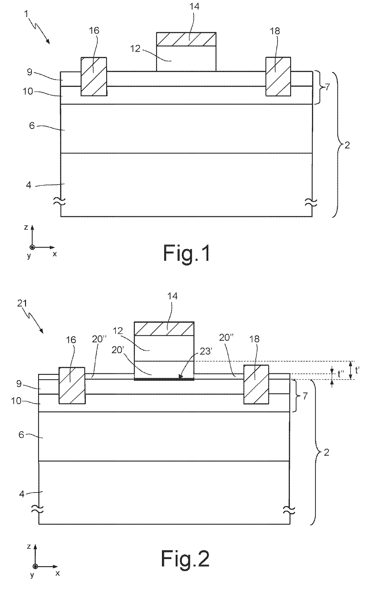
[0030]FIG. 2 is a schematic illustration of a HEMT 21 according to an embodiment of the present disclosure. In particular, FIG. 2 illustrates the HEMT 21 in a triad of mutually orthogonal axes x, y, z, in lateral sectional view in the plane xz. Elements of the HEMT 21 of FIG. 2 that are in common with the HEMT 1 of FIG. 1 are designated by the same reference numbers.

[0031]The HEMT 21 of FIG. 2 differs from the HEMT 1 of FIG. 1 for the presence of a diffusion-control region20′, made, for example, of gallium nitride, which extends on the heterostructure 7.

[0032]In particular, the diffusion-control region 20′ extends between the doped gate region 12 and the heterostructure 7, and has a thickness t′ comprised, for example, between 5 nm and 30 nm, for example 20 nm. In a top plan view of the HEMT 21, the doped gate region 12 and the auxiliary gate region 20′ are arranged on top of one another. In particular, the doped gate region 12 extends completely over, and in direct contact with, th...


PUM


Abstract

A manufacturing method of an HEMT includes: forming a heterostructure; forming a first gate layer of intrinsic semiconductor material on the heterostructure; forming a second gate layer, containing dopant impurities of a P type, on the first gate layer; removing first portions of the second gate layer so that second portions, not removed, of the second gate layer form a doped gate region; and carrying out a thermal annealing of the doped gate region so as to cause a diffusion of said dopant impurities of the P type in the first gate layer and in the heterostructure, with a concentration, in the heterostructure, that decreases as the lateral distance from the doped gate region increases.

Description

BACKGROUNDTechnical Field[0001]The present disclosure relates to a method of invention a high-electron-mobility transistor (HEMT) of a normally off type with reduced ON state resistance, and to a HEMT of a normally off type with reduced ON state resistance.Description of the Related Art[0002]Known to the art are HEMTs with a heterostructure, in particular of gallium nitride (GaN) and aluminum gallium nitride (AlGaN), at the interface of which a conductive channel may form, in particular a two-dimensional electron gas (2DEG) channel. For instance, HEMTs are appreciated for their use as high-frequency switches and as power switches, thanks to their high breakdown threshold and to the high electron mobility and density of charge carriers in their conductive channel. In addition, the high current density in the conductive channel of the HEMT affords a low ON state resistance (or simply RON) of the conductive channel.[0003]In HEMTs of a known type, in which a gate electrode extends over ...

Claims


Application Information

Patent Timeline
IPC IPC(8): H01L29/66H01L29/10H01L29/20H01L21/324H01L21/225H01L29/778
CPCH01L29/66462H01L29/1066H01L29/2003H01L21/3245H01L21/2258H01L29/778H01L29/0688H01L29/7786
Inventor IUCOLANO, FERDINANDO
Owner STMICROELECTRONICS SRL
Why Eureka
Try Eureka