Unlock instant, AI-driven research and patent intelligence for your innovation.

Active device array substrate and method for inspecting the same

a technology of active devices and array substrates, which is applied in the direction of static indicating devices, non-linear optics, instruments, etc., can solve the problems of low detection rate and inapparent image, and the problem of inapparent image or even no image is often encountered, and achieves the effect of increasing the detection rate of defects in active device array substrates

Active Publication Date: 2016-07-28
AU OPTRONICS CORP
View PDF8 Cites 3 Cited by
  • Summary
  • Abstract
  • Description
  • Claims
  • Application Information

AI Technical Summary

Benefits of technology

The invention allows for inspecting defects in a display area without damaging the driving circuit on the substrate. This is achieved by inputting a test signal to the tested signal line from the control line, resulting in an obvious infrared image. Additionally, the detection rate of defects in a GOA-type active device array substrate is increased.

Problems solved by technology

However, when a short position of the GOA-type active device array substrate is inspected, it often has problems of a low detection rate and inapparent image.
Particularly, taking an infrared heating location detection as an example, the problem of inapparent image or even no image is often encountered.
Moreover, since a test signal has to flow through a driving circuit around a display area before entering the display area, if intensity of the test signal is increased, the driving circuit probably withstands an excessive voltage or current to cause a damage.

Method used


Image

  • Active device array substrate and method for inspecting the same
  • Active device array substrate and method for inspecting the same
  • Active device array substrate and method for inspecting the same

Examples


Embodiment Construction

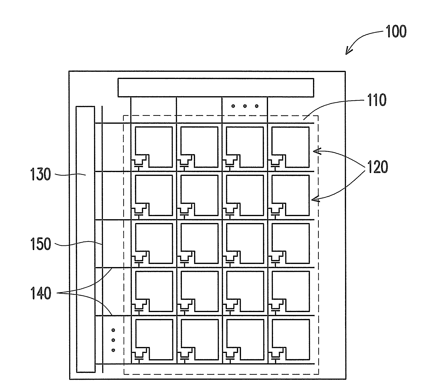
[0027]In the invention, by inputting a test signal to a tested signal line from a control line, an effect of inspecting a location of a defect in a display area is achieved without making the test signal to flow through a driving circuit, such that during the inspection, an infrared image is obvious produced without damaging the driving circuit on a gate on array (GOA)-type active device array substrate. In fact, the control line of the invention is, for example, a start pulse signal line, and the start pulse signal line is originally used for providing a start pulse signal Vst, and a gate signal is generated according to the start pulse signal Vst. In other words, the test signal can be transmitted by using the existing circuit on the substrate, such that the test signal can enter pixel structures in the display area without passing through the driving circuit on the GOA-type active device array substrate, and it is unnecessary to additionally form other lines to serve as the contr...


PUM


Abstract

An active device array substrate is provided. The active device array substrate includes multiple pixel structures, a drive circuit, multiple signal lines and a control line. The pixel structures are disposed in a display area. The drive circuit is disposed outside the display area. The signal lines are electrically connected to the drive circuit and the pixel structures corresponded to the signal lines. The control lines are intersected with the signal lines. A method adapted for inspecting defects on the active device array substrate is also provided. First, a tested signal line is selected from the signal lines, and the control line and the tested-signal line are conducted. Second, a test signal is input from the control line to the tested-signal line to determine a location of a defect. Finally, the control line and the tested signal line are isolated.

Description

CROSS-REFERENCE TO RELATED APPLICATION[0001]This application claims the priority benefit of Taiwan application serial no. 104102318, filed on Jan. 23, 2015. The entirety of the above-mentioned patent application is hereby incorporated by reference herein and made a part of this specification.BACKGROUND[0002]1. Technical Field[0003]The invention relates to a device array substrate and a method for inspecting the same, and particularly relates to an active device array substrate adapted to a display panel and a method for inspecting the same.[0004]2. Related Art[0005]Liquid crystal display panel is mainly composed of an active device array substrate, a color filter array substrate and a liquid crystal layer, where the active device array substrate includes a plurality of signal lines and a plurality of pixels arranged in an array, and the pixels are respectively connected to the corresponding signal lines. Generally, in order to avoid increasing a manufacturing cost, the industry tren...

Claims


Application Information

Patent Timeline
IPC IPC(8): G09G3/36
CPCG09G3/3611G09G2300/0426G09G2320/0693G02F1/1309G02F1/1362G09G3/006G02F1/136254G09G3/3648G09G2300/043G09G2330/10G09G2330/12
Inventor PAN, YING-HAO
Owner AU OPTRONICS CORP
Features
  • R&D
  • Intellectual Property
  • Life Sciences
  • Materials
  • Tech Scout
  • Unparalleled Data Quality
  • Higher Quality Content
  • 60% Fewer Hallucinations
Learn More