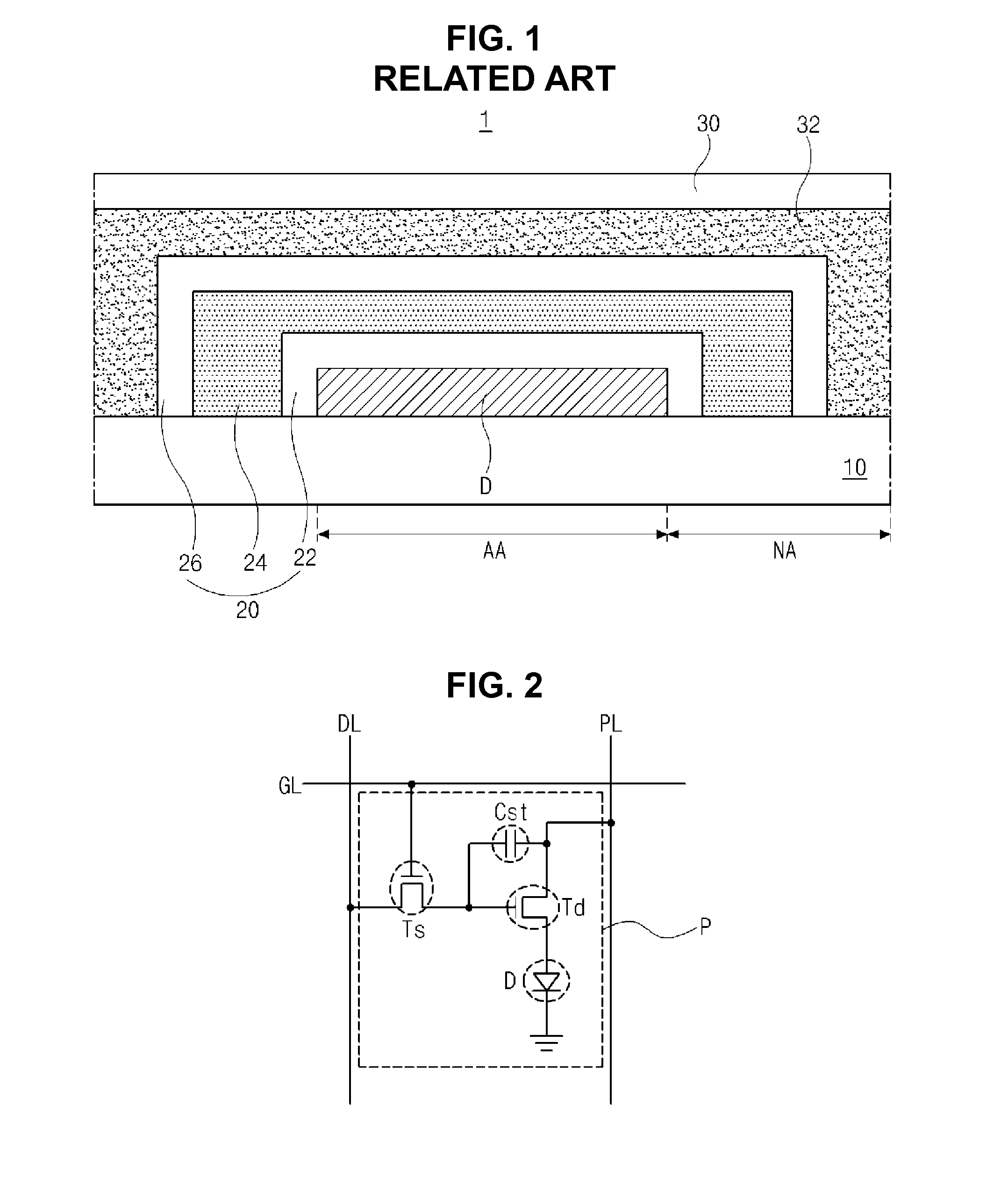
Flexible organic light emitting diode display device and method of fabricating the same
a light emitting diode and display device technology, applied in the direction of basic electric elements, semiconductor devices, electrical equipment, etc., can solve the problems of displaying quality and or lifetime of the related art oled display device, and still generated damage to the light emitting diode d
- Summary
- Abstract
- Description
- Claims
- Application Information
AI Technical Summary
Benefits of technology
Problems solved by technology
Method used
Image

Examples
first embodiment
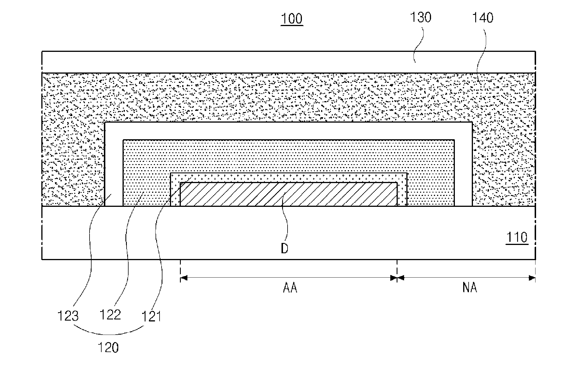
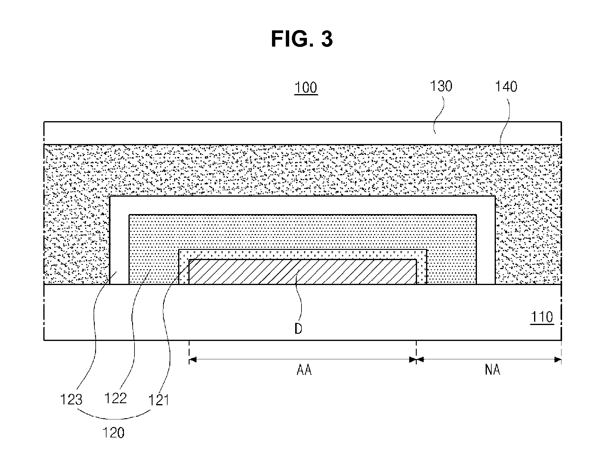
[0060]FIG. 3 is a schematic cross-sectional view of a flexible OLED display device according to the present invention, and FIG. 4 is a schematic cross-sectional view illustrating one pixel region including a light emitting diode.
[0061]As shown in FIGS. 3 and 4, a flexible OLED display device 100 according to the first embodiment of the present invention includes a flexible substrate 110, where a display area AA and a non-display area NA at peripheries of the display area AA are defined, a light emitting diode D on the flexible substrate 110, and an encapsulation film 120 covering the light emitting diode D, and a first inorganic layer 121 as a lowest layer of the encapsulation film 120 is formed by an atomic layer deposition (ALD) method.
[0062]The flexible substrate 110 may be formed of polymer such as polyimide. However, it is not limited thereto.
[0063]Although not shown, a buffer layer, which is formed of an inorganic insulating material, such as silicon oxide or silicon nitride, ...
second embodiment
[0098]FIG. 5 is a schematic cross-sectional view of a flexible OLED display device according to the present invention.
[0099]As shown in FIG. 5, a flexible OLED display device 200 according to the second embodiment of the present invention includes a flexible substrate 210, where a display area AA and a non-display area NA at peripheries of the display area AA are defined, a light emitting diode D on the flexible substrate 210 and an encapsulation film 220 covering the light emitting diode D and including a first inorganic sub-layer 221, a second inorganic sub-layer 222, an organic layer 223 and a second inorganic layer 224. The first inorganic layer includes the first inorganic sub-layer 221 and the second inorganic sub-layer 222. The first inorganic sub-layer 221 as a lowest layer of the encapsulation film 220 is formed by the ALD method, and the second inorganic sub-layer 222 on the first inorganic sub-layer 221 is formed by the PECVD method.
[0100]The flexible substrate 210 may be...
third embodiment
[0121]FIG. 6 is a schematic cross-sectional view of a flexible OLED display device according to the present invention.
[0122]As shown in FIG. 6, a flexible OLED display device 300 according to the third embodiment of the present invention includes a flexible substrate 310, where a display area AA and a non-display area NA at peripheries of the display area AA are defined, a light emitting diode D on the flexible substrate 310 and an encapsulation film 320 covering the light emitting diode D and including a first inorganic sub-layer 321, a second inorganic sub-layer 322, a first organic layer 323, a second inorganic layer 324 and a second organic layer 325. The second inorganic layer includes the first inorganic sub-layer 321 and the second inorganic sub-layer 322. The first inorganic sub-layer 321 as a lowest layer of the encapsulation film 320 is formed by the PECVD method, and the second inorganic sub-layer 322 on the first inorganic sub-layer 321 is formed by the ALD method.
[0123]...
PUM
 Abstract
Description
Claims
Application Information
 - R&D Engineer
- R&D Manager
- IP Professional
- Industry Leading Data Capabilities
- Powerful AI technology
- Patent DNA Extraction
Browse by: Latest US Patents, China's latest patents, Technical Efficacy Thesaurus, Application Domain, Technology Topic.
© 2024 PatSnap. All rights reserved.Legal|Privacy policy|Modern Slavery Act Transparency Statement|Sitemap