Manufacturing method of display substrate of display panel

A technology for display substrates and substrates, used in manufacturing tools, semiconductor/solid-state device manufacturing, semiconductor/solid-state device testing/measurement, etc., can solve the problems of narrow process window, expensive, time-consuming and cutting samples, etc., to prevent damage. , Reduced manufacturing cost, improved effect of adjustable process window

Inactive Publication Date: 2016-06-01
BOE TECH GRP CO LTD
View PDF4 Cites 16 Cited by
  • Summary
  • Abstract
  • Description
  • Claims
  • Application Information

AI Technical Summary

Problems solved by technology

[0006] However, the film on the substrate is usually very thin
Even slightly higher laser energies than required during the cutting process can cause damage to the layers to be exposed (e.g. TFT layers)
As a result, the process window can be relatively narrow using traditional laser cutting techniques
Also, adjusting the laser energy to the proper level can be time consuming and expensive to cut the sample
Furthermore, even if the laser energy level is set at a suitable value, a small fluctuation in energy may cause damage to the layer to be exposed (e.g., TFT layer)

Method used


Image

  • Manufacturing method of display substrate of display panel
  • Manufacturing method of display substrate of display panel
  • Manufacturing method of display substrate of display panel

Examples


Embodiment Construction

[0028] In order for those skilled in the art to better understand the technical solutions of the present invention, a display panel and a display device provided by the present invention will be further described in detail below with reference to the drawings and specific embodiments. Wherever possible, the same reference numbers will be used throughout the drawings to refer to the same or like parts.

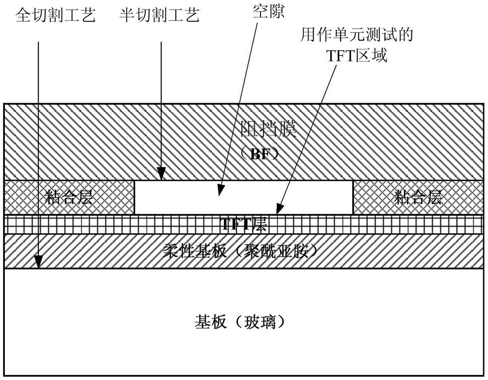
[0029] An aspect of the present invention provides a flexible OLED structure for a half-cut process.

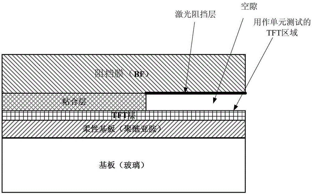
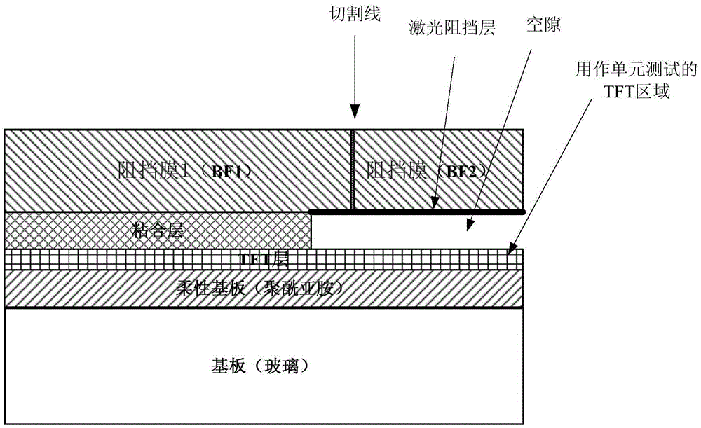
[0030] figure 1 A cross-sectional view of a portion of a flexible OLED structure for forming a flexible OLED display panel is shown. The flexible OLED structure may include a barrier film, an adhesive layer, a TFT layer, a flexible substrate and a rigid substrate. The rigid substrate, which may be made of glass, is used to support the flexible substrate and components formed on the flexible substrate during manufacturing and testing. The rigid substrate can be removed durin...


PUM

PropertyMeasurementUnit
thicknessaaaaaaaaaa
thicknessaaaaaaaaaa
wavelengthaaaaaaaaaa

Abstract

The invention provides a manufacturing method of a display substrate of a display panel. The method comprises: a flexible organic light emitting diode (OLED) substrate is provided; a thin-film transistor layer is arranged on the flexible OLED substrate; a bonding layer with patterns is arranged on the thin-film transistor layer which comprises at least one testing region; a blocking film is provided, and a laser blocking layer with patterns is arranged on a surface of the blocking film, the surface of the blocking film facing the thin-film transistor layer; the blocking film is bonded to the flexible OLED substrate, so that at least one part of the laser blocking layer is corresponding to the at least one testing region; a laser beam is used to irradiate the blocking film along the cutting line, so that a first part of the blocking film is removed from a second part of the blocking film.

Description

technical field [0001] The present invention relates to display technology, in particular, to a display panel for a display panel [0002] The manufacturing method of the substrate is shown. Background technique [0003] Organic light-emitting diode (organic light-emitting diode, OLED) devices are currently widely used. Among various OLED devices, manufacturers have shown great interest in flexible OLED devices and produced various flexible OLED devices. [0004] Such as figure 1 As shown, a flexible OLED display panel usually includes multiple films or layers, such as barrier film (barrier film, BF), organic layer (not shown), adhesive layer, thin-film transistor (thin-film transistor, TFT) layer, flexible substrate and substrate. During the fabrication of flexible OLED display panels, laser dicing is typically used to remove portions of one or more films on the substrate, exposing certain components on the substrate for testing. Carbon dioxide lasers have been commonl...

Claims


Application Information

Patent Timeline
Patent Type & Authority Applications(China)
IPC IPC(8): H01L27/12H01L21/66B23K26/14B23K26/38
CPCB23K26/14B23K26/38H01L22/30H01L27/1262H01L27/1218H01L27/1266H10K71/00H10K59/125H10K2102/311H01L21/76867
Inventor 刘陆谢明哲蔡宝鸣
Owner BOE TECH GRP CO LTD
Why Eureka
Try Eureka