OLED (organic light emitting diode) device package structure, OLED device and display screen

A technology of device packaging and components, which is applied in the field of OLED devices and display screens, and OLED device packaging structures, can solve problems such as uneven light output, different light output efficiency, and irregular microstructure, and achieve high total reflection and uniform light output.

Active Publication Date: 2017-02-22
WUHAN CHINA STAR OPTOELECTRONICS TECH CO LTD
View PDF4 Cites 15 Cited by
  • Summary
  • Abstract
  • Description
  • Claims
  • Application Information

AI Technical Summary

Problems solved by technology

However, the microstructure formed by the OLED device material itself is generally irregular, so that the light extraction efficiency of different positions of the OLED device is different, resulting in uneven light output.

Method used


Image

  • OLED (organic light emitting diode) device package structure, OLED device and display screen
  • OLED (organic light emitting diode) device package structure, OLED device and display screen
  • OLED (organic light emitting diode) device package structure, OLED device and display screen

Examples


Embodiment Construction

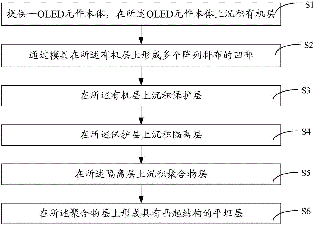
[0022] The following will clearly and completely describe the technical solutions in the embodiments of the present invention with reference to the drawings in the embodiments of the present invention. The described embodiments are only some, not all, embodiments of the present invention. Based on the embodiments of the present invention, other embodiments obtained by persons of ordinary skill in the art without making creative efforts all belong to the protection scope of the present invention.

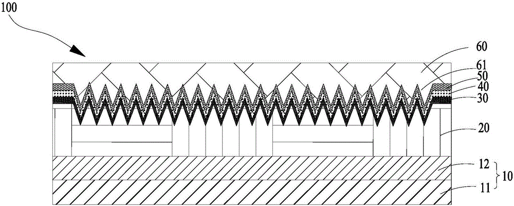
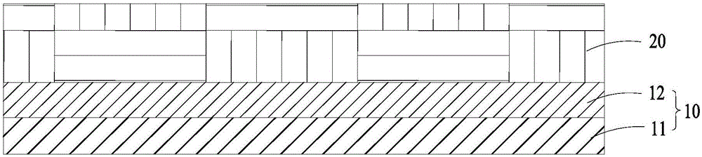
[0023] see figure 1 , the OLED device packaging structure provided by the present invention is used on the OLED device 100 . The OLED device 100 can be either a rigid OLED device or a flexible OLED device. The OLED device 100 includes an OLED element body 10 and an encapsulation layer (not shown in the figure). The encapsulation layer includes an organic layer 20 , a protection layer 30 , a barrier layer 40 , a stress layer 50 and a flat layer 60 .

[0024] The OLED element body ...


PUM


Abstract

The invention provides an OLED (organic light emitting diode) device package structure and a method for manufacturing the same. The method includes forming an organic layer with regular array structures on an OLED component by the aid of mold plates with array protrusions; sequentially forming a protective layer, a barrier layer, a stress layer and a flat layer by the aid of further deposition processes; forming protrusions with regular array structures on the flat layer. The OLED device package structure and the method have the advantages that internal total reflection effects and micro-cavity resonance effects of an OLED device can be reduced by the aid of refraction effects of the protrusions and various film layers, and accordingly the light emergent efficiency of the OLED device can be improved; the protective layer can protect the array structures of the organic layer against being damaged; the barrier layer can prevent the OLED device from being eroded by water and oxygen, and accordingly the quality of the OLED device can be further improved; the OLED device can be normally used even in certain curled and bent states owing to the stress layer.

Description

technical field [0001] The invention relates to the technical field of OLEDs, in particular to an OLED device packaging structure, an OLED device and a display screen. Background technique [0002] When the light generated inside the OLED device propagates inside, due to the mismatch of the optical coefficients (such as the refractive index) of each material interface, there will be reflection, refraction and total reflection, which will greatly affect the external surface of the OLED device. Light efficiency. [0003] At present, the methods to improve the light extraction rate (light extraction) mainly include setting microstructures inside the OLED device, thereby reducing total reflection and adjusting the cavity resonance effect of the OLED device to improve the light extraction efficiency. However, the microstructure formed by the material of the OLED device itself is generally irregular, so that the light extraction efficiency at different positions of the OLED devic...

Claims


Application Information

Patent Timeline
Patent Type & Authority Applications(China)
IPC IPC(8): H01L51/52
CPCH10K50/852H10K50/854H10K50/844
Inventor 黄金昌徐湘伦
Owner WUHAN CHINA STAR OPTOELECTRONICS TECH CO LTD
Why Eureka
Try Eureka