Display apparatus having pattern of slits on top-common electrode

a display apparatus and common electrode technology, applied in non-linear optics, instruments, optics, etc., can solve the problems of affecting display quality, deterioration of rate and reliability, etc., and achieve the effect of improving product conformity and improving display quality of display apparatus

Active Publication Date: 2017-02-02
INNOLUX CORP
View PDF7 Cites 7 Cited by
  • Summary
  • Abstract
  • Description
  • Claims
  • Application Information

AI Technical Summary

Benefits of technology

[0007]The disclosure is directed to a display apparatus. Through special pattern design of slits on the common electrode formed over the pixel electrode layer, display quality of the display apparatus is improved and becomes more stable, and product conformity rate is increased.

Problems solved by technology

If the display apparatus has poor design, both conformity rate and reliability will deteriorate, and display quality will be affected.

Method used


Image

  • Display apparatus having pattern of slits on top-common electrode
  • Display apparatus having pattern of slits on top-common electrode
  • Display apparatus having pattern of slits on top-common electrode

Examples


first embodiment

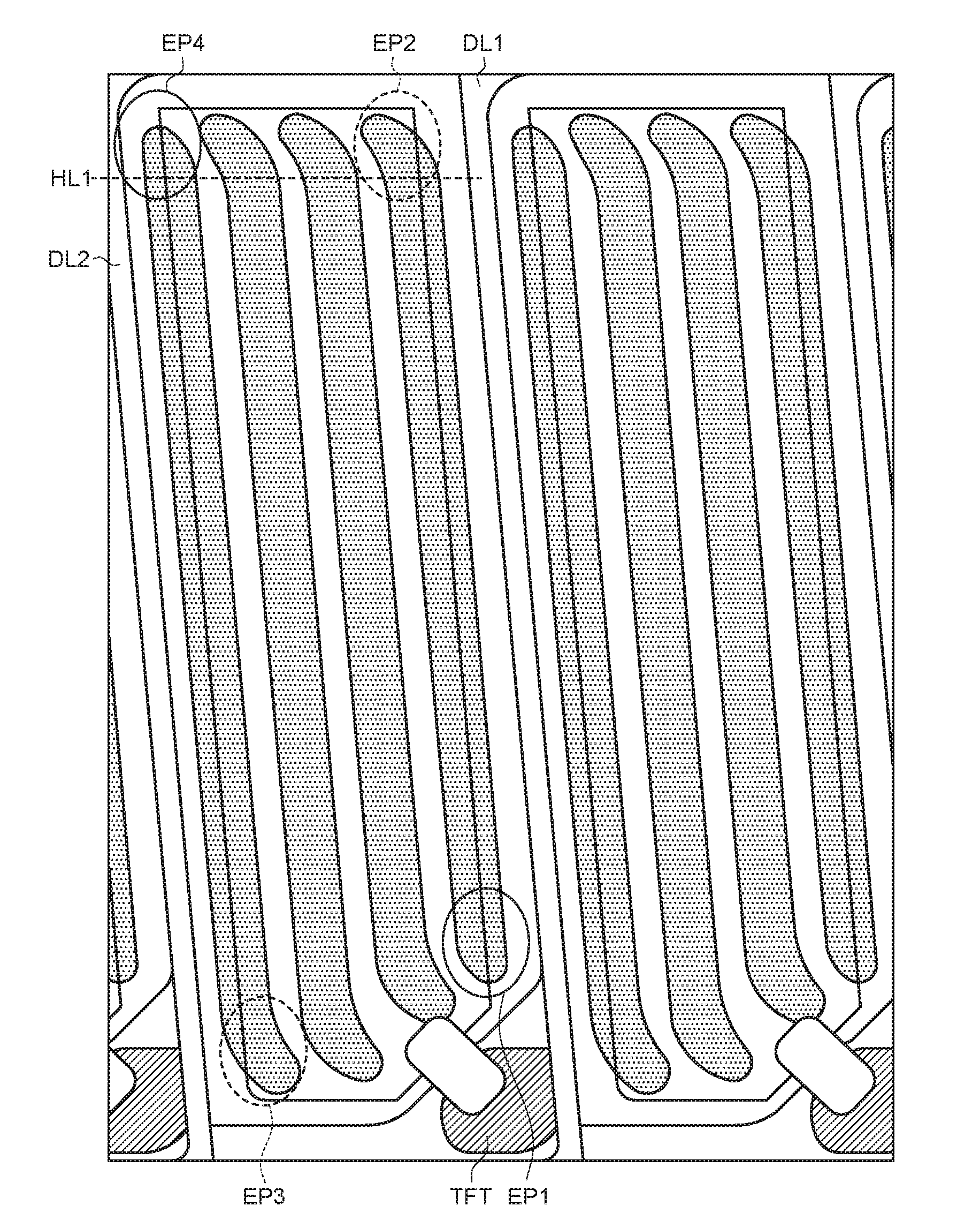
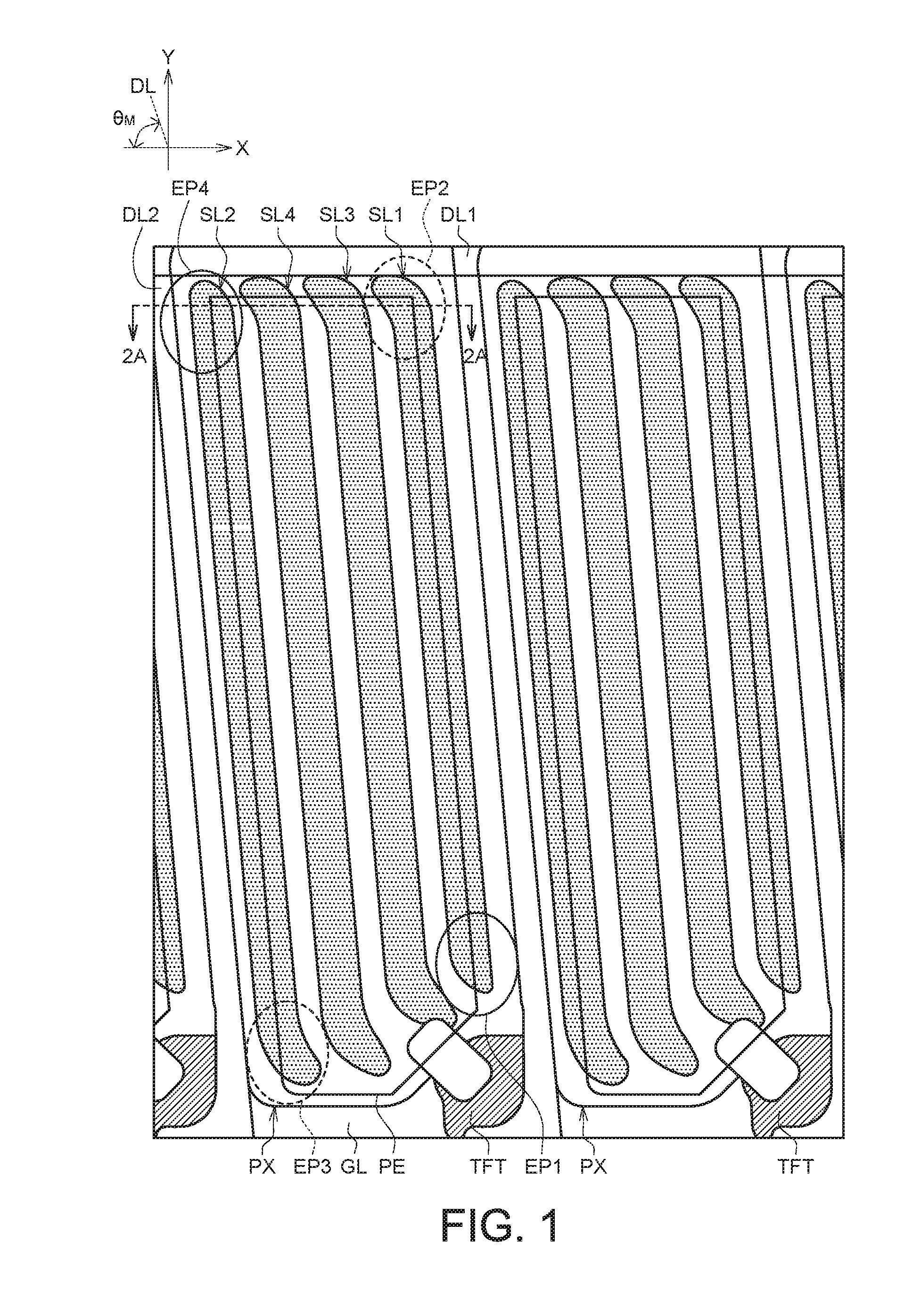
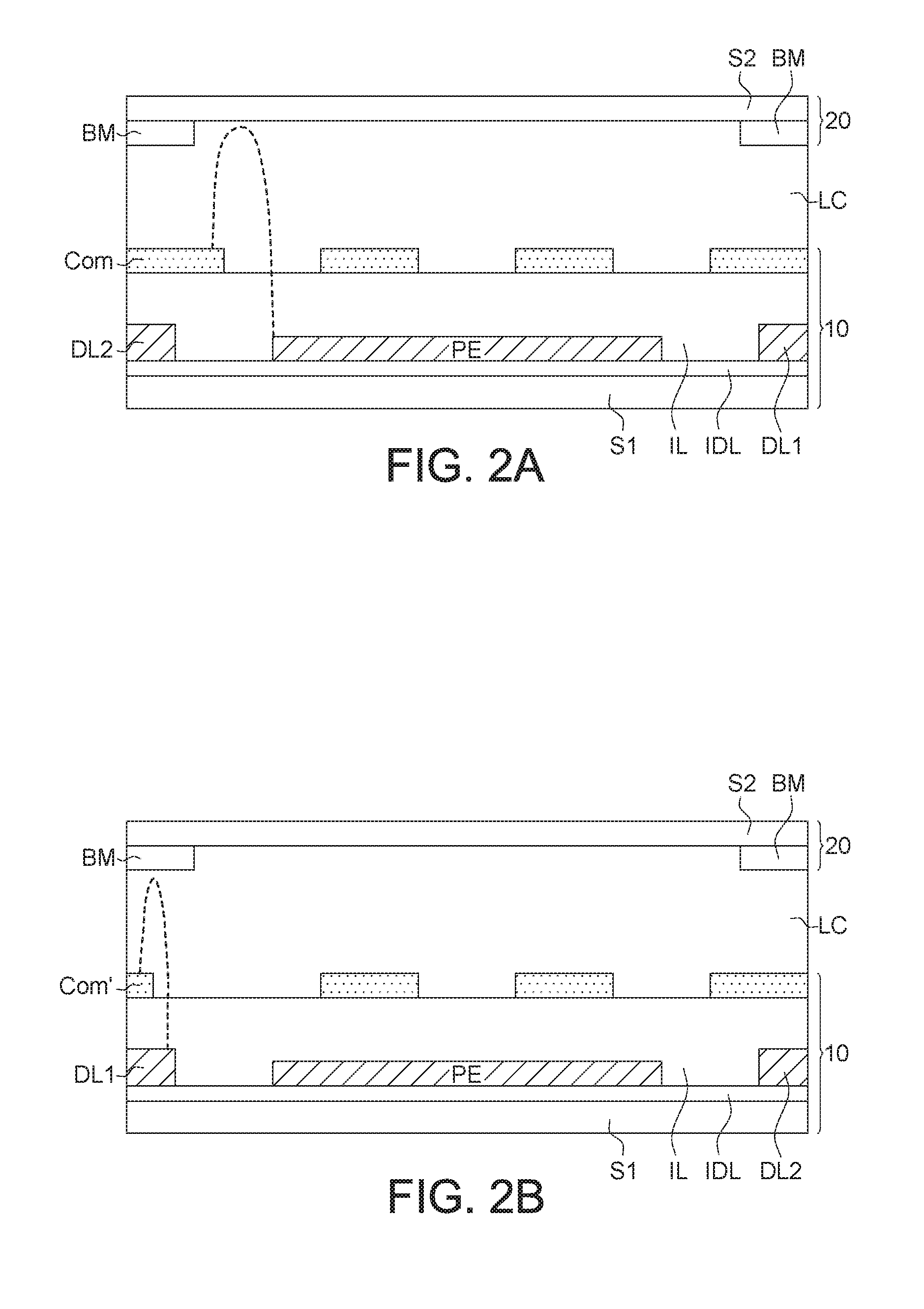
[0027]FIG. 1 shows a top view of two adjacent pixels of a display apparatus according to a first embodiment of the present disclosure. FIG. 2A shows a cross-sectional view of a pixel of a display apparatus along a cross-sectional line 2A-2A of FIG. 1. In the first embodiment, a display apparatus includes a first substrate 10, a second substrate 20, and a display medium (such as a liquid crystal LC) disposed between the first substrate and the second substrate (FIG. 2A). The first substrate 10 and the second substrate 20 can be realized by such as an array substrate (such as a thin-film transistor (TFT) substrate) and a color filter (CF) substrate respectively. In an embodiment as indicated in FIG. 1, the first substrate 10 includes a first base plate S1, and a plurality of gate lines GL and a plurality of data lines DL formed on the first base plate S1, wherein two adjacent data lines (such as the first data line DL1 and the second data line DL2) intersect with the gate line GL to d...

second embodiment

[0031]FIG. 3 shows a top view of two adjacent pixels of a display apparatus according to a second embodiment of the present disclosure. The second embodiment and the first embodiment have the same design of slit end portions of the common electrode layer (the same reference numerals are used for the same components). For example, of the first slit SL1 nearest to the first data line DL1, the first end portion EP1 adjacent to the gate line GL does not have a bend; of the second slit SL2 nearest to the second data line DL2, the fourth end portion EP4 away from the gate line GL does not have a bend either. Other remaining end portions of the slits have the bend. Details of the components are described with reference to the first embodiment, and are not repeated here. The first embodiment and the second embodiment mainly differ in the shape of the pixel.

[0032]In the first embodiment, the pixel is a parallelogram, and the angle θM formed by the data line (such as the first data line DL1, ...

third embodiment

[0035]FIG. 4A and FIG. 4B respectively show a top view of two adjacent pixels of a display apparatus according to a third embodiment of the present disclosure. The two adjacent pixels respectively have 3 slits and 2 slits in a pixel region. The design of slit end portions of the common electrode layer is the same in the third embodiment and the first embodiment. The same reference numerals are used for the same components. For example, of the first slit SL1 nearest to the first data line DL1, the first end portion EP1 adjacent to the gate line GL does not have a bend; of the second slit SL2 nearest to the second data line DL2, the fourth end portion EP4 away from the gate line GL does not have a bend either. Other remaining end portions of the slits have the bend. The first end portion EP1 and the fourth end portion EP4 have different quantities of slits. Details are described in the first embodiment, and are not repeated here. Furthermore, the pixel PX illustrated in FIG. 4A and FI...


PUM

PropertyMeasurementUnit
angleaaaaaaaaaa
obtuse angleaaaaaaaaaa
angle θ4aaaaaaaaaa

Abstract

A display apparatus, including a first substrate, a second substrate and a display medium, is provided. The first substrate includes a gate line, a first data line and a second data line. The first data line and the second data line intersect with the gate line to define a pixel including a pixel electrode layer and a common electrode layer. The common electrode layer at least includes a first slit having first and second end portions, and a second slit having third and fourth end portions. A largest distance from the edge of the first end portion near the first data line to the first data line is defined as a first distance. A largest distance from the edge of the second end portion near the first data line to the first data line is defined as a second distance, which is larger than the first distance.

Description

[0001]This application claims the benefit of People's Republic of China application Serial No. 201510454606.7, filed Jul. 29, 2015, the subject matter of which is incorporated herein by reference.BACKGROUND OF THE INVENTION[0002]Field of the Invention[0003]The disclosure relates in general to a display apparatus, and more particularly to a display apparatus having pattern of slits on a common electrode formed over a pixel electrode layer.[0004]Description of the Related Art[0005]Nowadays, electronic products with display panel have become indispensable necessities to modern people in their everyday life, work, study, and entertainment. Examples of electronic products include smart phones, PC tablets, notebooks, monitors and TVs. Of the above electronic products, display apparatus with liquid crystal display (LCD) panel is most popular. Particularly, LCD apparatus, having the advantages of simple application, lightweight, portability, lower cost, higher reliability, and being friendl...

Claims


Application Information

Patent Timeline
Patent Type & Authority Applications(United States)
IPC IPC(8): G02F1/1343G02F1/1368G02F1/1362
CPCG02F1/134309G02F1/136286G02F2001/134318G02F2201/121G02F2201/123G02F1/1368G02F1/134318G02F1/133707G02F1/134372
Inventor YANG, SHUN-CHENHSU, YU-LUNLIN, YING-TONG
Owner INNOLUX CORP
Why Eureka
Try Eureka