Fully Depleted Silicon On Insulator Flash Memory Design

a technology of silicon on insulator and flash memory, which is applied in the direction of digital storage, electrical equipment, instruments, etc., can solve the problem that the design of fully depleted silicon on insulator transistors has not been used in flash memory systems

Active Publication Date: 2017-04-06
SILICON STORAGE TECHNOLOGY
View PDF6 Cites 9 Cited by
  • Summary
  • Abstract
  • Description
  • Claims
  • Application Information

AI Technical Summary

Problems solved by technology

To date, fully depleted silicon-on-insulator trans...

Method used


Image

  • Fully Depleted Silicon On Insulator Flash Memory Design
  • Fully Depleted Silicon On Insulator Flash Memory Design
  • Fully Depleted Silicon On Insulator Flash Memory Design

Examples


Embodiment Construction

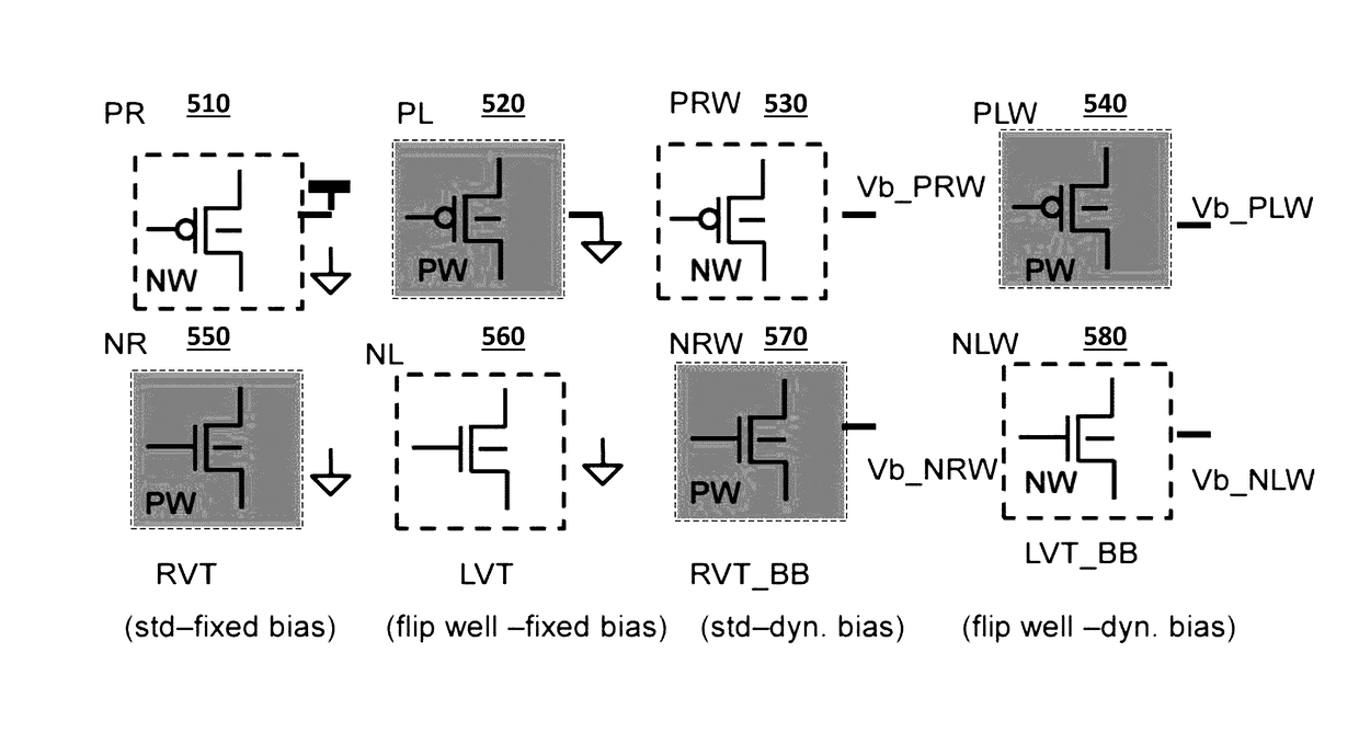
[0044]FIG. 5 depicts eight FDSOI transistor types that are used in the embodiments described herein.

[0045]Standard fixed bias FDSOI MOS transistors includes PMOS transistor 510 and NMOS transistor 550. FDSOI PMOS transistor 510 comprises an n-well that is biased to Vdd power supply and optionally to ground, in this case transistor channel length is modified to have similar threshold voltage level. FDSOI NMOS transistor 550 comprises a p-well that is biased to ground. The PMOS 510 and NMOS 550 are regular threshold voltage devices.

[0046]Flipped well fixed bias FDSOI MOS transistors includes PMOS transistor 520 and NMOS transistor 560. FDSOI PMOS transistor 520 comprises a p-well that is biased to ground. FDSOI NMOS transistor 560 comprises an n-well that is biased to ground. The PMOS 520 and NMOS 560 are low threshold voltage devices, i.e., its threshold voltage is lower than that of the PMOS 510 and NMOS 550.

[0047]Standard dynamic bias FDSOI MOS transistors includes PMOS transistor ...


PUM


Abstract

The present invention relates to a flash memory system wherein one or more circuit blocks utilize fully depleted silicon-on-insulator transistor design to minimize leakage

Description

TECHNICAL FIELD[0001]The present invention relates to a flash non-volatile memory system wherein one or more circuit blocks utilize fully depleted silicon-on-insulator transistor design to minimize leakage and optimize performance.BACKGROUND OF THE INVENTION[0002]A prior art non-volatile memory cell 110 is shown in FIG. 1. The memory cell 110 comprises a semiconductor substrate 112 of a first conductivity type, such as P type. The substrate 112 has a surface on which there is formed a first region 114 (also known as the source line SL) of a second conductivity type, such as N type. A second region 116 (also known as the drain line) also of N type is formed on the surface of the substrate 112. Between the first region 114 and the second region 116 is a channel region 118. A bit line BL 120 is connected to the second region 116. A word line WL 122 is positioned above a first portion of the channel region 118 and is insulated therefrom. The word line 122 has little or no overlap with t...

Claims


Application Information

Patent Timeline
IPC IPC(8): G11C16/14G11C16/26G11C16/08
CPCG11C16/14G11C16/26G11C16/08G11C16/16G11C7/065G11C8/08G11C16/10G11C16/28G11C2216/04H01L28/00H10B43/27H10B20/00
Inventor TRAN, HIEU VANLY, ANHVU, THUANNGUYEN, HUNG QUOC
Owner SILICON STORAGE TECHNOLOGY
Why Eureka
Try Eureka