Amoled pixel driving circuit and pixel driving method

a driving circuit and pixel technology, applied in the field of display technology, can solve the problems of complex alternating current power supply voltage vdd, no compensation function of traditional 2t1c pixel driving circuit, etc., and achieve the effect of reducing the complexity of the power supply voltage signal

Inactive Publication Date: 2017-05-18
SHENZHEN CHINA STAR OPTOELECTRONICS TECH CO LTD
View PDF15 Cites 7 Cited by
  • Summary
  • Abstract
  • Description
  • Claims
  • Application Information

AI Technical Summary

Benefits of technology

[0007]An objective of the present invention is to provide an AMOLED pixel driving circuit, which can effectively compensate the

Problems solved by technology

However, the traditional 2T1C pixel driving circuit has no compensation function.
However, drawbacks of compl

Method used


Image

  • Amoled pixel driving circuit and pixel driving method
  • Amoled pixel driving circuit and pixel driving method
  • Amoled pixel driving circuit and pixel driving method

Examples


Embodiment Construction

[0079]For better explaining the technical solution and the effect of the present invention, the present invention will be further described in detail with the accompanying drawings and the specific embodiments.

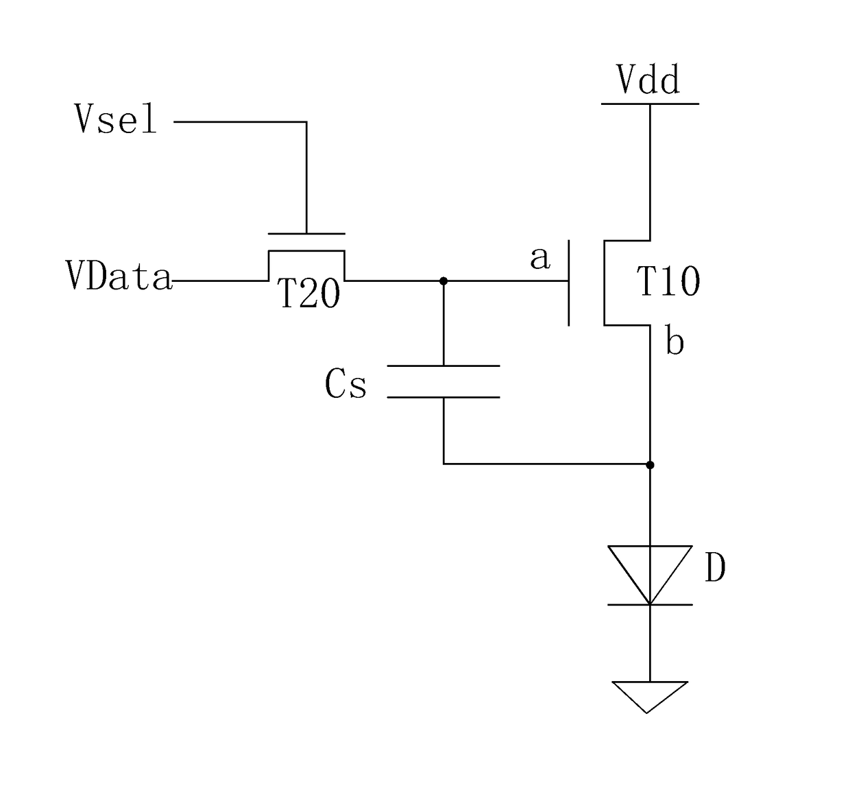
[0080]Please refer to FIG. 3. The present invention first provides an AMOLED pixel driving circuit, and the AMOLED pixel driving circuit comprises: a first thin film transistor T1, a second thin film transistor T2, a third thin film transistor T3, a storage capacitor Cs and an organic light emitting diode OLED.

[0081]a gate of the first thin film transistor T1 is electrically coupled to a first node a, and a source is electrically coupled to a second node b, and a drain is electrically coupled to a power supply voltage Vdd;

[0082]a gate of the second thin film transistor T2 is electrically coupled to a first scan signal voltage Vsel1, and a source is electrically coupled to a data signal voltage VData, and a drain is electrically coupled to the first node a;

[0083]a gate of the t...


PUM


Abstract

The present invention provides an AMOLED pixel driving circuit and a pixel driving method. The AMOLED pixel driving circuit utilizing the 3T1C structure comprises: a first thin film transistor (T1), a second thin film transistor (T2), a third thin film transistor (T3), a storage capacitor (Cs) and an organic light emitting diode (OLED), and the second scan signal voltage (Vsel2) in introduced. The third thin film transistor (T3) provides initial low voltage level (Vini) of the data signal voltage (VData) to the source of the first thin film transistor (T1), i.e. the drive thin film transistor in the reset stage, which can effectively compensate the threshold voltage changes of the drive thin film transistor for diminishing the complexity of the power supply voltage signal.

Description

FIELD OF THE INVENTION[0001]The present invention relates to a display technology field, and more particularly to an AMOLED pixel driving circuit and a pixel driving method.BACKGROUND OF THE INVENTION[0002]The Organic Light Emitting Display (OLED) possesses many outstanding properties of self-illumination, low driving voltage, high luminescence efficiency, short response time, high clarity and contrast, near 180° view angle, wide range of working temperature, applicability of flexible display and large scale full color display. The OLED is considered as the most potential display device.[0003]The OLED can be categorized into two major types according to the driving methods, which are the Passive Matrix OLED (PMOLED) and the Active Matrix OLED (AMOLED), i.e. two types of the direct addressing and the Thin Film Transistor (TFT) matrix addressing. The AMOLED comprises pixels arranged in array and belongs to active display type, which has high lighting efficiency and is generally utiliz...

Claims


Application Information

Patent Timeline
IPC IPC(8): G09G3/3258H01L27/12H01L27/32G09G3/3266G09G3/3291
CPCG09G3/3258G09G3/3266G09G3/3291H01L27/3262G09G2330/021H01L27/1225H01L27/124H01L27/3276G09G2300/0819H01L27/1255G09G3/3233G09G2300/0842H10K59/131H10K59/1213
Inventor CAI, YUYING
Owner SHENZHEN CHINA STAR OPTOELECTRONICS TECH CO LTD
Why Eureka
Try Eureka