Display device and method for driving same

a display device and matrix-type technology, applied in the field of display devices, can solve the problems of reducing the luminance of pixels of the display device with usage time, and achieve the effects of preventing a reduction in the image quality of the display image, reducing power consumption of the display device, and simplifying the configuration of the scanning line drive circui

Active Publication Date: 2017-06-29
SHARP KK
View PDF3 Cites 50 Cited by
  • Summary
  • Abstract
  • Description
  • Claims
  • Application Information

AI Technical Summary

Benefits of technology

[0166]According to the first or thirty-ninth aspect of the present invention, when pause driving is performed using a drive period and a pause period, a current measurement period is set in the pause period, and a current outputted from a pixel circuit to which a measurement voltage has been written can be measured in the current measurement period. In addition, by writing a data voltage to the pixel circuit in the current measurement period, an influence exerted on a display image by the current measurement is suppressed, enabling to prevent a reduction in the image quality of the display image.
[0167]According to the second aspect of the present invention, by fixing the voltages of the scanning lines during a period other than the current measurement period in the pause period, power consumption of the display device can be reduced.
[0168]According to the third aspect of the present invention, by generating, using the same shift register, a scanning signal for the drive period and a scanning signal for the pause period based on an enable signal that changes in different manners for the drive period and the pause period, the configuration of the scanning line drive circuit can be simplified.
[0169]According to the fourth aspect of the present invention, a scanning signal based on the enable signal can be outputted separately from an output signal to the subsequent stage using two output control circuits.
[0170]According to the fifth aspect of the present invention, a first output control circuit that outputs an output signal to the subsequent stage can be configured using a first output control transistor, and a second output control circuit that outputs a scanning signal can be configured using a second output control transistor.
[0171]According to the sixth aspect of the present invention, a display device including: pixel circuits, each including an electro-optical element, three transistors, and a capacitor; and monitoring lines can measure currents in the pixel circuits while preventing a reduction in the image quality of a display image using simple circuits.

Problems solved by technology

The organic EL display device has a problem of a reduction in the luminances of pixels with usage time.

Method used


Image

  • Display device and method for driving same
  • Display device and method for driving same
  • Display device and method for driving same

Examples


fourth embodiment

4. Fourth Embodiment

[0351]

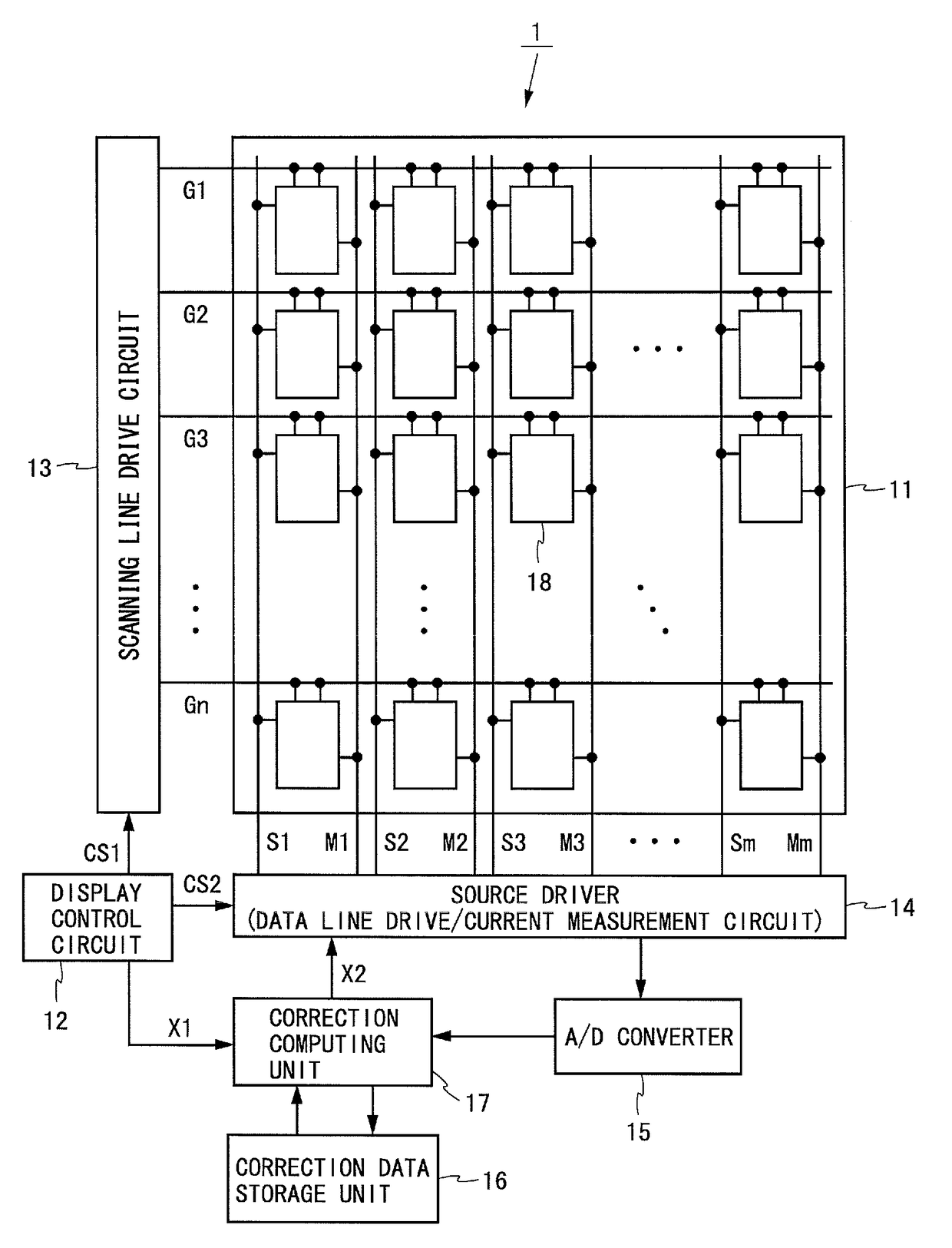
[0352]An overall configuration of a display device, a configuration of pixel circuits, a configuration of a scanning line drive circuit, and a configuration of unit circuits are the same as those of the third embodiment, and thus, description thereof is omitted (see FIGS. 20 to 23). The display device according to the present embodiment differs from the display device according to the third embodiment in drive method. Specifically, in the third embodiment, pause driving is adopted, and current measurement for characteristic detection (characteristic detection for a drive transistor or an organic EL) is performed in a pause period. In the present embodiment, on the other hand, pause driving does not necessarily need to be adopted, and current measurement for characteristic detection is performed in a normal display period.

[0353]

[0354]FIG. 26 is a timing chart for describing a drive method of the present embodiment. It is assumed that current measurement (cur...

fifth embodiment

5. Fifth Embodiment

[0366]

[0367]FIG. 27 is a block diagram showing a configuration of a display device according to a fifth embodiment of the present invention. A display device 4 shown in FIG. 27 is such that a power supply unit 19 is added to the display device 3 according to the third embodiment. The display device 4 according to the present embodiment differs from the display device 3 according to the third embodiment in drive method. Specifically, in the third embodiment, pause driving is adopted and current measurement for characteristic detection is performed in a pause period. In the present embodiment, on the other hand, current measurement for characteristic detection is performed at power-on or power-off. More specifically, a dedicated period for performing current measurement is provided immediately after a power-on button of the display device 3 is pressed or immediately after a power-off button of the display device 3 is pressed.

[0368]A source driver 14 functionally inc...

first embodiment

[0424]A method for driving an active matrix-type display device having a display unit including a plurality of scanning lines, a plurality of data lines, a plurality of monitoring lines, and a plurality of pixel circuits arranged two-dimensionally; and having a drive period and a pause period, the method including:

[0425]a step of driving the plurality of scanning lines; and

[0426]a step of driving the plurality of data lines and measuring currents outputted from the respective pixel circuits, wherein

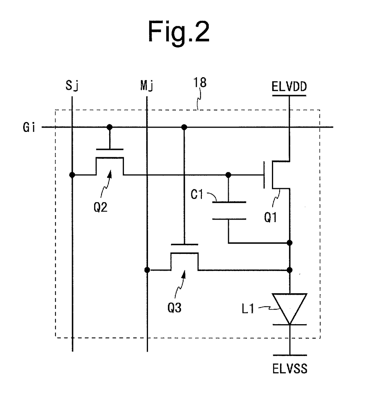
[0427]each of the pixel circuits includes:[0428]an electro-optical element;[0429]a drive transistor provided in series with the electro-optical element;[0430]a write control transistor provided between a corresponding data line and a control terminal of the drive transistor, and having a control terminal connected to a corresponding scanning line;[0431]a read control transistor provided between a corresponding monitoring line and one conductive terminal of the drive transistor, and having...


PUM


Abstract

In a current measurement period set in a pause period, a display device of the present invention applies measurement voltages to data lines (S1 to Sm) and measures currents outputted to monitoring lines (M1 to Mm) from m pixel circuits (18), and then applies data voltages generated corresponding to video signals to the data lines (S1 to Sm).

Description

TECHNICAL FIELD[0001]The present invention relates to a display device, and more particularly to an active matrix-type display device including electro-optical elements such as organic EL elements, and a method for driving the display device.BACKGROUND ART[0002]In recent years, as a thin, lightweight, and fast responsible display device, attention has been focused on an organic EL (Electro Luminescence) display device. The organic EL display device includes a plurality of pixel circuits arranged two-dimensionally. Each pixel circuit of the organic EL display device includes an organic EL element and a drive transistor provided in series with the organic EL element. The drive transistor controls the amount of current flowing through the organic EL element, and the organic EL element emits light at a luminance depending on the amount of current flowing therethrough.[0003]The organic EL display device has a problem of a reduction in the luminances of pixels with usage time. The reason ...

Claims


Application Information

Patent Timeline
Patent Type & Authority Applications(United States)
IPC IPC(8): G09G3/3258G09G3/3291G11C19/28G09G3/3266
CPCG09G3/3258G09G3/3266G09G3/3291G11C19/28G09G2330/12G09G2310/08G09G2320/045G09G2320/048G09G2330/023G09G2310/0286G09G3/3233G09G2300/0842G09G2310/065G09G2320/0285G09G2320/0295G09G2330/027G09G2330/026G09G2230/00G09G2320/0214
Inventor NISHIKAWA, DAICHIOGAWA, YASUYUKIYAMAMOTO, KAORUKISHI, NORITAKAYAMANAKA, SHIGETSUGUOHARA, MASANORINOGUCHI, NOBORU
Owner SHARP KK
Why Eureka
Try Eureka