Chip and electronic device

a technology of electronic devices and chips, applied in the field of electronic devices, can solve the problems of poor quality of electronic devices, instability of the operation of the chip in the electronic device, damage, etc., and achieve the effect of reducing or eliminating the damage of electrostatics and protecting stability when the chip is functioning

Inactive Publication Date: 2017-06-29
TCL CHINA STAR OPTOELECTRONICS TECH CO LTD
View PDF1 Cites 1 Cited by
  • Summary
  • Abstract
  • Description
  • Claims
  • Application Information

AI Technical Summary

Benefits of technology

[0014]Compared with prior art, the chip of the present invention and the chip in the electronic device having the chip comprises at least one ESD protection circuit, and the ESD protection circuit can reduce or eliminate the damage of electrostatic to other elements or circuit inside the chip, and thus to protect the stability when the chip is functioning. Furthermore, the ESD protection circuit of the chip according to the present invention is located inside the chip, and setting the ESD protection circuit outside the chip is not required. Compared with the condition that the ESD protection circuit is set outside the chip, the ESD protection circuit of the present invention is located inside the chip, and thus, the function of the chip is further integrated to avoid the trouble of being externally coupled to the ESD protection circuit when using.

Problems solved by technology

Triboelectrification and human body electrostatic are two great harms in the electronics industry, which often cause the operation instability of the chip in the electronic device, or even damage.
Thus, it results in poor quality of electronic device.

Method used


Image

  • Chip and electronic device
  • Chip and electronic device
  • Chip and electronic device

Examples


Embodiment Construction

[0019]Embodiments of the present invention are described in detail with the technical matters, structural features, achieved objects, and effects with reference to the accompanying drawings as follows. It is clear that the described embodiments are part of embodiments of the present invention, but not all embodiments. Based on the embodiments of the present invention, all other embodiments to those of ordinary skill in the premise of no creative efforts obtained, should be considered within the scope of protection of the present invention.

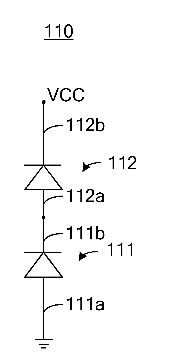
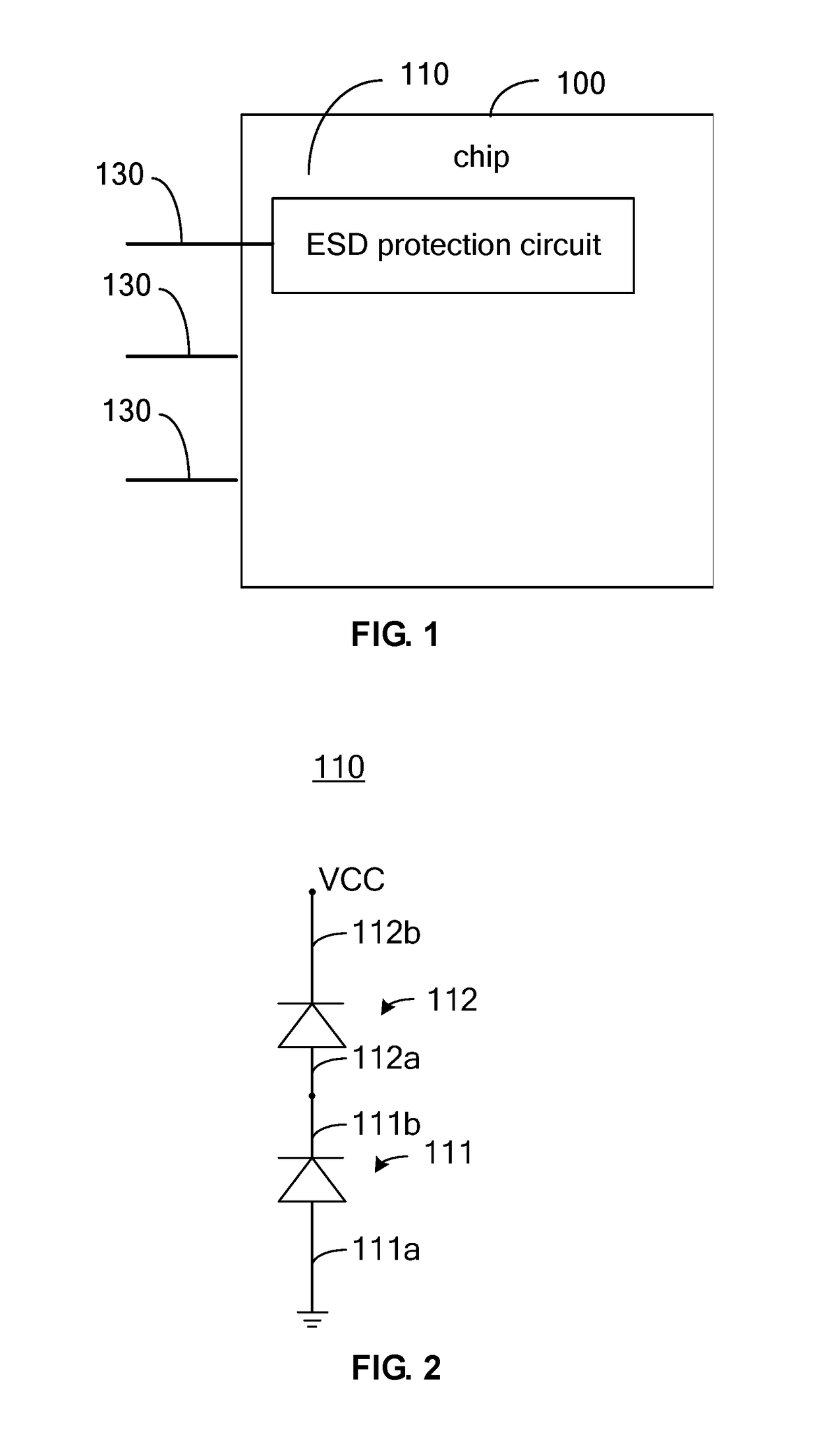
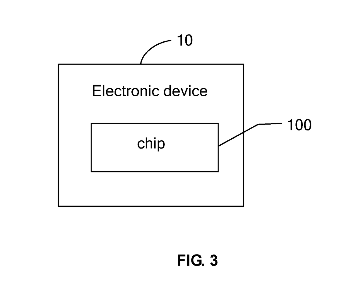
[0020]Please refer to FIG. 1 and FIG. 2, together. FIG. 1 is a circuit structure diagram of a chip according to the preferred embodiment of the present invention. FIG. 2 is a circuit diagram of an ESD protection circuit in a chip according to the preferred embodiment of the present invention. The chip 100 can be located in the electronic device. The electronic device comprises the smart phone, the mobile internet device (MID), the electronic book, ...


PUM


Abstract

The present invention provides a chip and an electronic device. The chip comprises at least one pin, and the chip comprises at least one ESD (Electrostatic Discharge) protection circuit inside, and the ESD protection circuit is employed to reduce or eliminate a damage of electrostatic to other elements or circuit inside the chip, and the ESD protection circuit is located corresponding to a pin, and the ESD protection circuit is electrically coupled to the pin. The electronic device comprises the aforesaid chip.

Description

CROSS REFERENCE[0001]This application claims the priority of Chinese Patent Application No. 2015010484331.1, entitled “Chip and electronic device”, filed on Aug. 7, 2015, the disclosure of which is incorporated herein by reference in its entirety.FIELD OF THE INVENTION[0002]The present invention relates to an electronic technology field, and more particularly to a chip and an electronic device.BACKGROUND OF THE INVENTION[0003]The electrostatic is a kind of objective existence of natural phenomena, there are many to produce it, such as contact, friction, electric induction, etc. The characteristic of the electrostatic is long time accumulation, high voltage, low power, small current and short time action. With the factors of the body's own actions or contact with other objects, separation, friction or induction, it can produce the electrostatic of several thousand volts or even tens of thousands of volts. Triboelectrification and human body electrostatic are two great harms in the el...

Claims


Application Information

Patent Timeline
Patent Type & Authority Applications(United States)
IPC IPC(8): H02H9/04H01L27/02
CPCH01L27/0255H02H9/046
Inventor ZHANG, XIANMINGCHEN, YU-YEHCHEN, MING-WEICAO, DAN
Owner TCL CHINA STAR OPTOELECTRONICS TECH CO LTD
Why Eureka
Try Eureka