
Pixel compensation circuit and method for driving the same, display panel and display device

a compensation circuit and display panel technology, applied in the field of electroluminescence, can solve the problems of inability to display frames with low grey scale, etc., and achieve the effect of improving uneven display of display panels and low grey scal

Inactive Publication Date: 2017-07-06
BOE TECH GRP CO LTD
View PDF6 Cites 11 Cited by
  • Summary
  • Abstract
  • Description
  • Claims
  • Application Information

AI Technical Summary

Benefits of technology

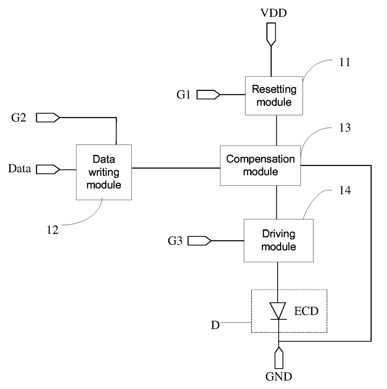
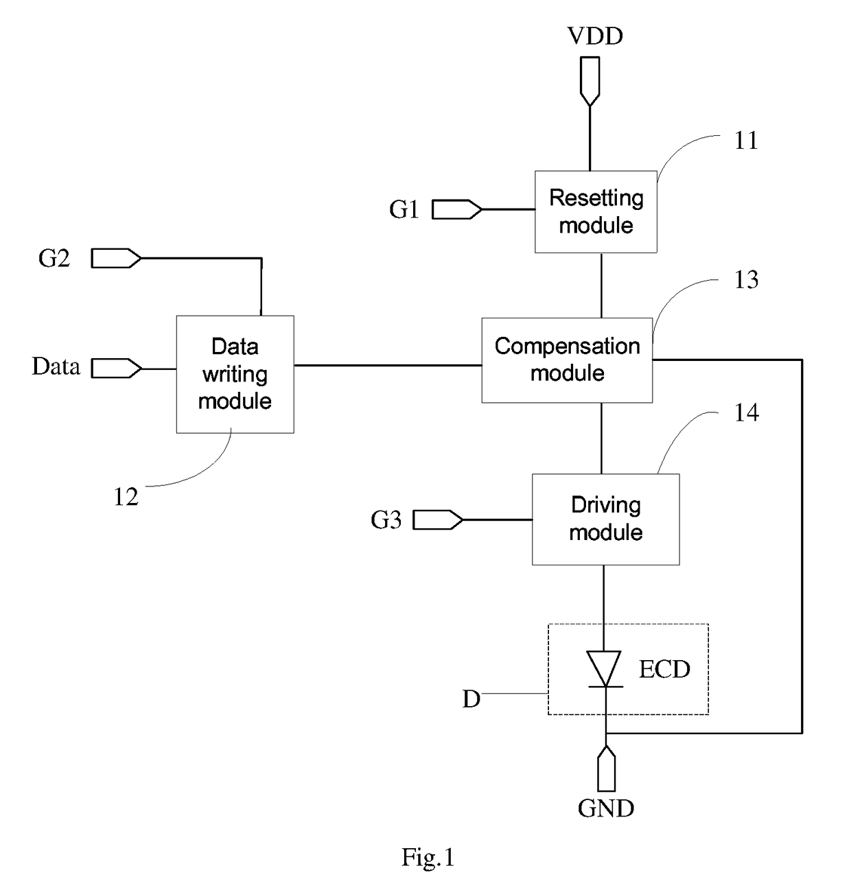
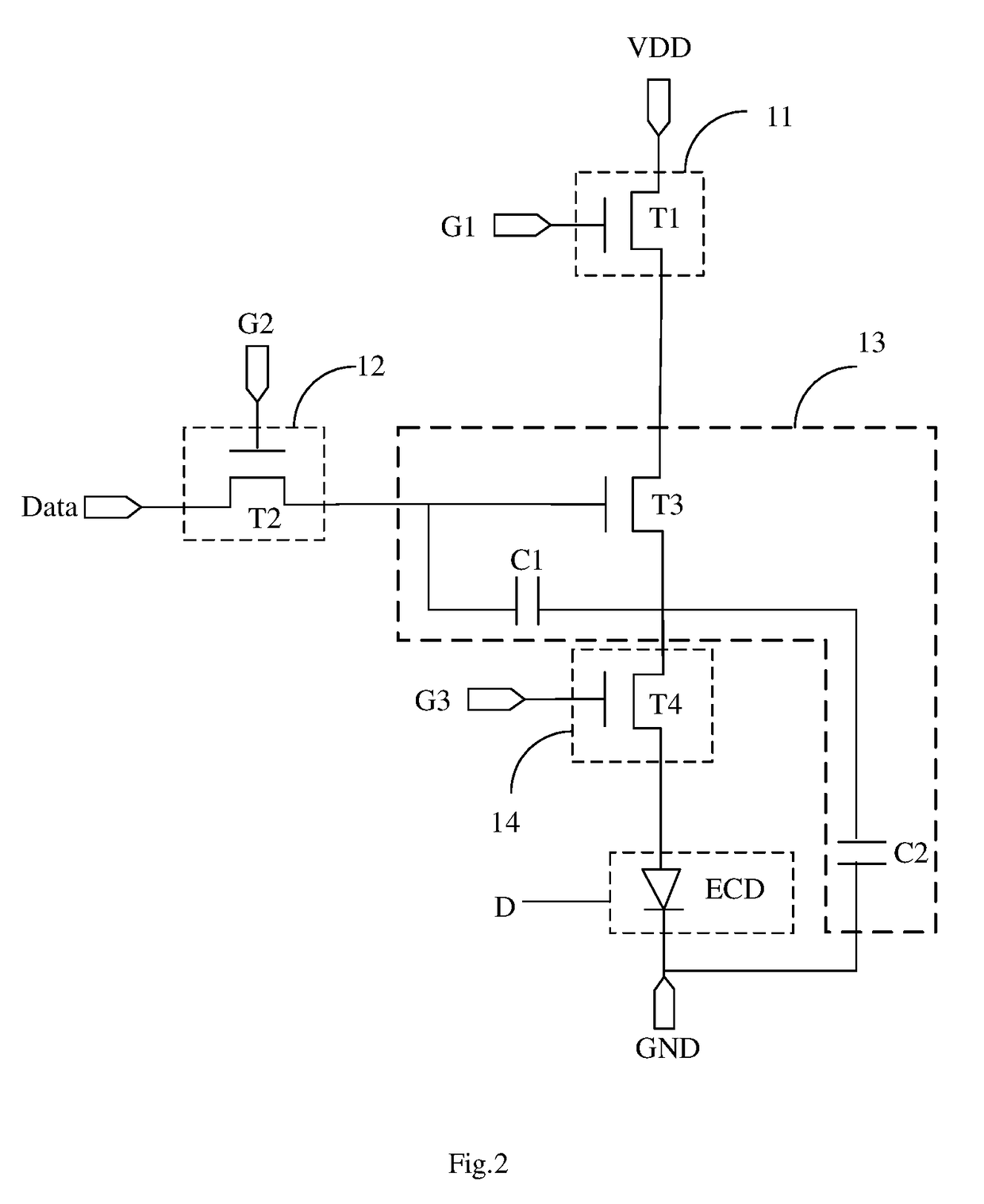
The present invention provides a pixel compensation circuit and method for driving the same, a display panel, and a display device that solves the problem of instability of voltages supplied to the light emitting device caused by different threshold voltage by cooperative operations of the respective modules of the pixel compensation circuit. This results in improving uneven displaying of the display panel and being capable of displaying frames with low grey scale by the display panel.

Problems solved by technology

However, due to voltage characteristic and capacitance characteristic of ECD light emitting device, when a conventional display driving method is utilized to drive the light emitting device, different threshold voltage Vth in the driving circuit may lead to instability of voltages supplied to the light emitting device, thereby resulting in uneven displaying of the display panel and being incapable of displaying frames with low grey scale.

Method used


Image

  • Pixel compensation circuit and method for driving the same, display panel and display device
  • Pixel compensation circuit and method for driving the same, display panel and display device
  • Pixel compensation circuit and method for driving the same, display panel and display device

Examples


Embodiment Construction

[0024]The technical solutions of the embodiments of the present disclosure will be described clearly and completely below in conjunction with accompanying drawings of the present disclosure. Obviously, the embodiments described are merely a part of embodiments of the present disclosure instead of all embodiments. All other embodiments obtained by an ordinary skilled in the art based on the embodiments of the present disclosure without contributing any creative labor should belong to the protection scope of the present disclosure.

[0025]The embodiment of the present disclosure provides a pixel compensation circuit and method for driving the same, a display panel and a display device which may solve the technical problem of instability of voltages supplied to the light emitting device caused by different threshold voltage Vth, thereby improving uneven displaying of the display panel and being capable of displaying frames with low grey scale by the display panel.

[0026]In conjunction wit...


PUM


Abstract

An embodiment of the present disclosure provides a pixel compensation circuit and method for driving the same, a display panel and a display device. The pixel compensation circuit comprises a resetting module, a data writing module, a compensation module, a driving module and a light emitting device. The embodiment of the present disclosure may prevent from issues of instability of voltage caused by different threshold voltages by cooperative operations of the respective modules of the pixel compensation circuit. When the light emitting device is controlled by the driving module to display, the difference value between a threshold voltage as well as a voltage difference between the control terminal of the compensation module and the output terminal of the compensation module is irrespective of the threshold voltage, so that the voltage supplied to the light emitting device will not be affected by the threshold voltage. Thus, the embodiment of the present disclosure provides a pixel compensation circuit to solve the technical problem of instability of voltages supplied to the light emitting device caused by different threshold voltage Vth, thereby improving uneven displaying of the display panel and being capable of displaying frames with low grey scale by the display panel.

Description

[0001]This application claims priority to Chinese Application No. 201610006982.4, filed on Jan. 5, 2016, entitled “PIXEL COMPENSATION CIRCUIT AND METHOD FOR DRIVING THE SAME, DISPLAY PANEL AND DISPLAY DEVICE”, which is incorporated herein by reference in their entireties.FIELD OF INVENTION[0002]The present invention relates to a technical field of electroluminescence field, especially to a pixel compensation circuit and method for driving the same, a display panel and display device.DESCRIPTION OF PRIOR ART[0003]With development of science and technology, there are much more types of display devices. With economic progress, it is focused on saving of energy. Thus, the present display products play attention to issues of power consumption. Electro chromic Device (ECD) is paid attention to by researchers for its low power consumption, low cost, self-illumination, wide view angle, rapid response speed and so on. For example, since ECD has a character of not-consuming power and transpar...

Claims


Application Information

Patent Timeline
IPC IPC(8): G09G3/20G09G3/38
CPCG09G3/2018G09G3/38G09G2300/0819G09G2310/027G09G2310/061G09G2320/0626G09G2300/0426G09G3/2077G09G2300/0852G09G2300/0861G09G2310/0262G09G2320/0233
Inventor WANG, YU
Owner BOE TECH GRP CO LTD
Learn More