Wiring structure and printed wiring substrate of wiring structure

a wiring structure and substrate technology, applied in the direction of printed circuit aspects, printed circuit non-printed electric components association, cross-talk/noise/interference reduction, etc., can solve the problems of increasing crosstalk noise, difficult to dispose of wirings in a small wiring substrate, and generating crosstalk noise, so as to reduce the crosstalk noise between the wiring patterns and reduce the capacitive coupling and inductive coupling

Active Publication Date: 2017-07-27
ALPINE ELECTRONICS INC
View PDF1 Cites 0 Cited by
  • Summary
  • Abstract
  • Description
  • Claims
  • Application Information

AI Technical Summary

Benefits of technology

[0019]In a wiring structure and a printed wiring substrate of the disclosure, the wiring space in a second direction can be made narrow by reducing an interval between the wiring patterns in a parallel wiring portion. In addition, the interval between the wiring patterns can be widened in a wiring path change portion. Therefore, a capacitive coupling and an inductive coupling between the wiring patterns can be reduced, and the crosstalk noise between the wiring patterns can be reduced.

Problems solved by technology

Therefore, when a digital signal is applied to the wiring pattern, a crosstalk noise is generated between the wiring patterns, and the crosstalk noise is increased as a transmission rate becomes higher.
Therefore, there is a need to provide a wide space for the wirings in a direction perpendicular to the extending direction of the wirings, and thus it is difficult to dispose the wirings in a small wiring substrate.
In addition, since there is a difference caused in the wiring length due to the one wiring extending in the straight line shape and the other wiring which is bent, these wirings are not suitable to a circuit design such as a high-speed interface which requires a timing control.

Method used


Image

  • Wiring structure and printed wiring substrate of wiring structure
  • Wiring structure and printed wiring substrate of wiring structure
  • Wiring structure and printed wiring substrate of wiring structure

Examples


first embodiment

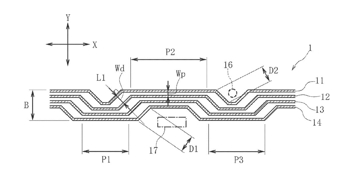
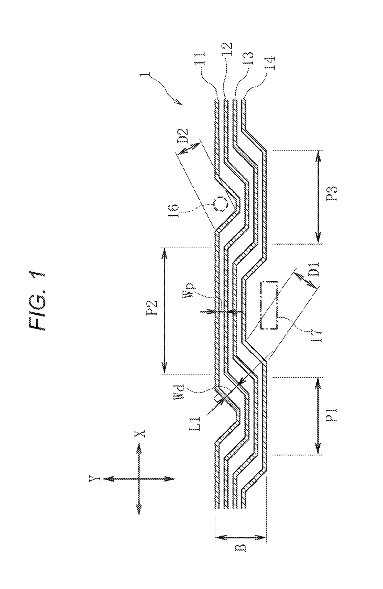
[0027]FIG. 1 illustrates a plan view of a wiring structure 1 of the disclosure. The wiring structure 1 is formed on the surface of a hard substrate or a flexible substrate to form a printed wiring substrate. In each drawing, an X direction represents a first direction, and a Y direction perpendicular to the X direction represents a second direction.

[0028]The wiring structure 1 includes a plurality of wiring patterns 11, 12, 13, and 14. The wiring patterns 11, 12, 13, and 14 are made of a conductive metal layer such as a copper foil.

[0029]The wiring structure 1 illustrated in FIG. 1 includes a first parallel wiring portion P1, a second parallel wiring portion P2, and a third parallel wiring portion P3. In the first parallel wiring portion P1, the second parallel wiring portion P2, and the third parallel wiring portion P3, at least two of the wiring patterns 11, 12, 13, and 14 are disposed to be linearly extended or paralleled to each other in the first direction (X direction). An int...

third embodiment

[0040]FIG. 4 illustrates a wiring structure 3 of the disclosure. In the wiring structure 3, the interval Wp between the wiring patterns 11, 12, and 13 in the parallel wiring portion is the same as those of the above embodiments. In a wiring path change portion D5, the respective wiring patterns 11, 12, and 13 are bent at a right angle.

[0041]Even in the wiring structure 3, the crosstalk noise can be reduced without increasing the width dimension in the Y direction.

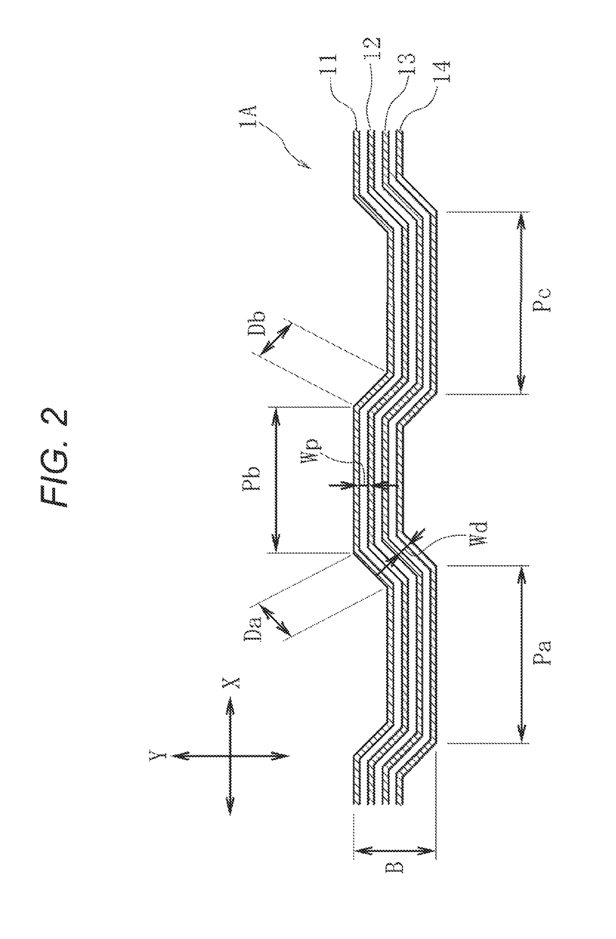
[0042]FIG. 5 illustrates a part of a printed wiring substrate 20 on which the wiring structure 1 illustrated in FIG. 1 is applied.

[0043]The printed wiring substrate 20 includes a plurality of wiring patterns 21 in the surface of a hard or flexible substrate. In the wiring structure, there are provided the parallel wiring portions P10 and P11 and a wiring path change portion D11. In the wiring path change portion D11, the respective wiring patterns are extended at a slope intersecting with the first direction, and the wiring...


PUM


Abstract

A wiring structure includes a plurality of wiring patterns. An interval between the adjacent wiring patterns is shortened in the parallel wiring portions. In wiring path change portions, the wiring patterns are extended at a slope with respect to an X direction, and an interval between the adjacent wiring patterns is more widened than the interval. A crosstalk noise can be reduced by widening the interval between the wiring patterns using the wiring path change portions without making an area occupied by a wiring region extremely increased.

Description

RELATED APPLICATION[0001]The present application claims priority to Japanese Patent Application Number 2016-011391, filed Jan. 25, 2016, the entirety of which is hereby incorporated by reference.BACKGROUND[0002]1. Field[0003]The present disclosure relates to a wiring structure of a wiring pattern which is formed on a hard substrate or a flexible substrate, and a printed wiring substrate of the wiring structure.[0004]2. Description of Related Art[0005]A plurality of wiring patterns are formed on a printed wiring substrate which is provided in an electronic apparatus, and the wiring patterns tend to be densely disposed when the electronic apparatus is miniaturized. When the wiring patterns are densely disposed in parallel to each other, there may cause a capacitive coupling due to a mutual capacitance and an inductive coupling due to a mutual inductance between the adjacent wiring patterns. Therefore, when a digital signal is applied to the wiring pattern, a crosstalk noise is generat...

Claims


Application Information

Patent Timeline
Patent Type & Authority Applications(United States)
IPC IPC(8): H05K1/02H05K1/18H05K1/11
CPCH05K1/0228H05K1/115H05K2201/09272H05K2201/09236H05K1/181H05K1/0216H05K1/116H05K2201/0245H05K2201/09263
Inventor IIDAKA, KENJI
Owner ALPINE ELECTRONICS INC
Why Eureka
Try Eureka