Substrate with built-in functional element

Inactive Publication Date: 2013-04-11
NEC CORP
View PDF5 Cites 11 Cited by
  • Summary
  • Abstract
  • Description
  • Claims
  • Application Information

AI Technical Summary

Benefits of technology

[0026]According to the present invention, it is possible provide a substrate with a built-in functional element, including the functional elem

Problems solved by technology

In addition, in a conventional wiring circuit substrate, signal wirings in the same layer are close to each other, and crosst

Method used


Image

  • Substrate with built-in functional element
  • Substrate with built-in functional element
  • Substrate with built-in functional element

Examples


first exemplary embodiment

[0048]A first invention of the present invention is described below by way of an exemplary embodiment.

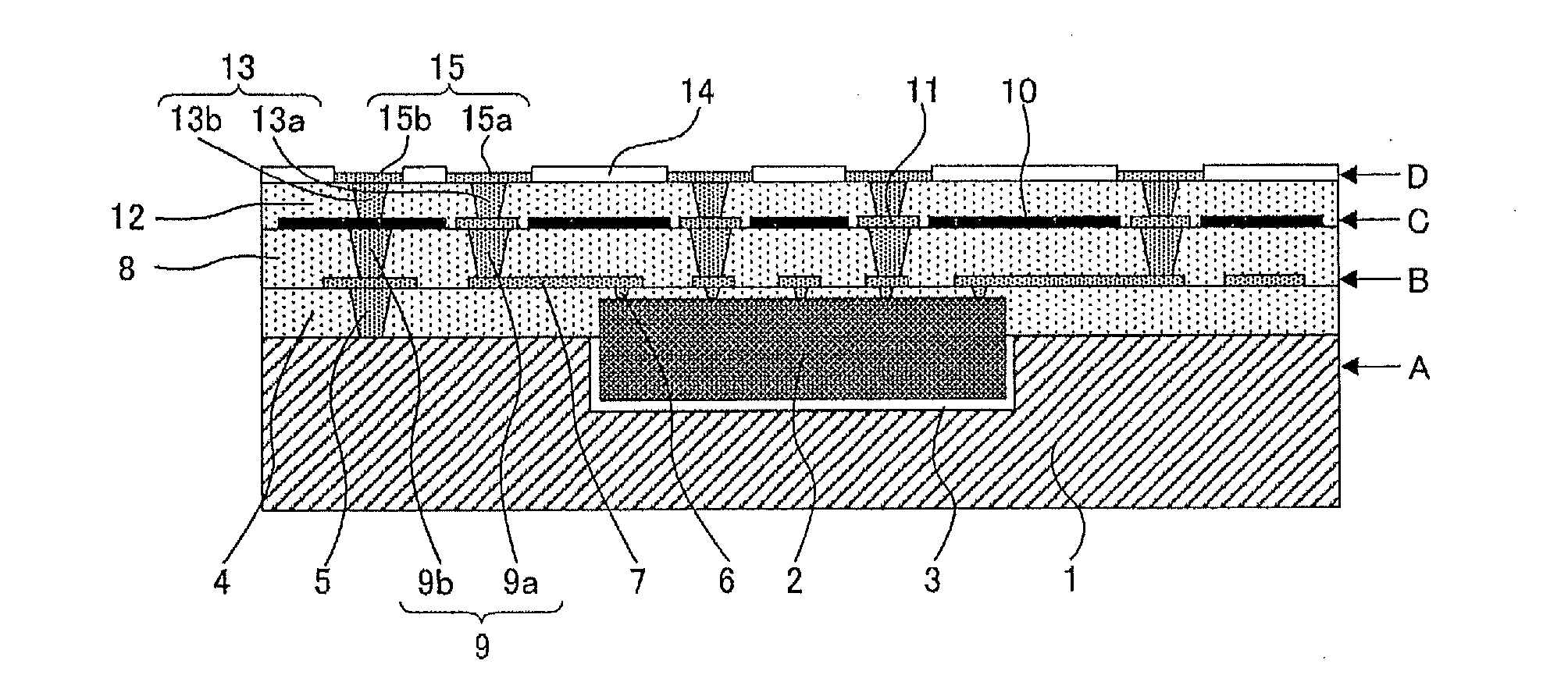
[0049]FIG. 1 illustrates a configuration example of a substrate with a built-in functional element according to the present exemplary embodiment. FIG. 1 is an outline cross-sectional view schematically illustrating a structure of the substrate with a built-in functional element according to the present exemplary embodiment.

[0050]In FIG. 1, a metal plate 1 that functions as a ground and a support is provided with a concave portion, and a functional element 2 such as a semiconductor chip is placed in the concave portion with the intermediation of an adhesive agent 3. The functional element 2 includes electrode terminals (not illustrated) on a circuit-side (the upper side of FIG. 1) surface thereof, and is placed above the metal plate 1 with the circuit surface thereof facing upward. The metal plate 1 supports the functional element 2, and is bonded to a rear-side (the lower side of FI...

second exemplary embodiment

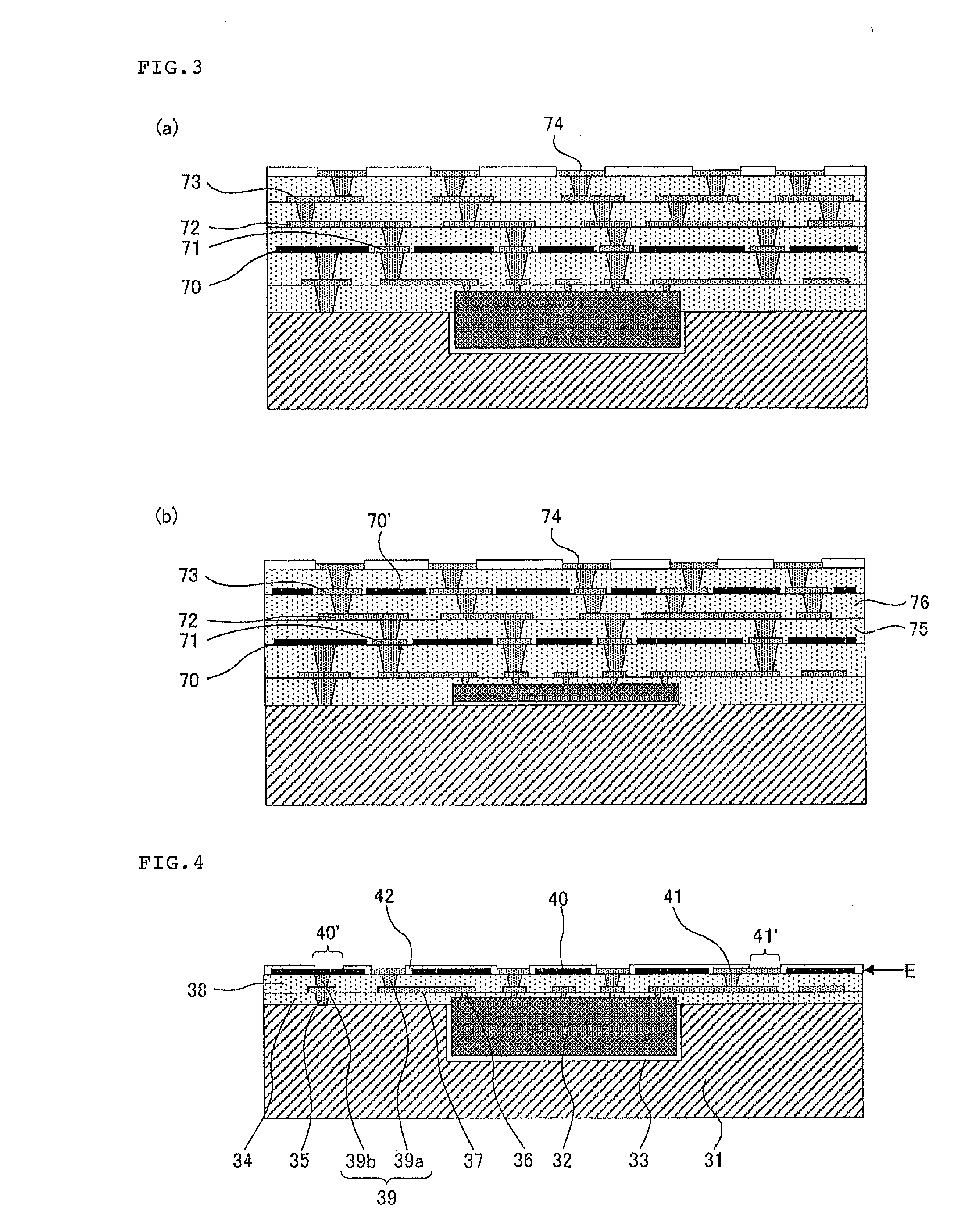
[0110]A second invention of the present invention is described below by way of an exemplary embodiment.

[0111]FIG. 5 illustrates a configuration example of a substrate with a built-in functional element according to the present exemplary embodiment. FIG. 5 is an outline cross-sectional view schematically illustrating a structure of the substrate with a built-in functional element according to the present exemplary embodiment. In FIG. 5, a functional element 102 such as a semiconductor chip is provided above a metal plate 101 that functions as a ground and a support, with the intermediation of an adhesive agent 103. The functional element 102 includes electrode terminals (not illustrated) on a circuit-side (the upper side of FIG. 5) surface thereof, and is placed above the metal plate 101 with the circuit surface thereof facing upward. The metal plate 101 supports the functional element 102, and is bonded to a rear-side (the lower side of FIG. 5) surface of the functional element 102 ...


PUM


Abstract

The present invention has an object to provide a substrate with a built-in functional element, including the functional element above a metal plate, in which crosstalk noise between signal wirings can be reduced and higher characteristic impedance matching can be achieved. An aspect of the present invention provides a substrate with a built-in functional element, including: a metal plate that includes a concave portion and serves as a ground; the functional element that is placed in the concave portion and includes an electrode terminal; a first insulating layer that covers the functional element and is placed in contact with the metal plate; a first wiring layer including first signal wiring that is opposite the metal plate with the first insulating layer being interposed therebetween; a second insulating layer that covers the first wiring layer; and a ground layer formed of a ground plane that is opposite the first wiring layer with the second insulating layer being interposed therebetween.

Description

TECHNICAL FIELD[0001]The present invention relates to a substrate with a built-in functional element, including one or more built-in functional elements such as semiconductor chips and an electronic device including the substrate with a built-in functional element.BACKGROUND ART[0002]Along with increasing demand for a higher information processing capacity, the operation of a semiconductor element is sped up, and the number of switchings is increased, so that signal wiring is required to have improved electrical characteristics, for example, matched characteristic impedance and reduction in crosstalk noise with another signal wiring. Consequently, in order to deal with such a demand, according to Patent Literature 1, the wiring structure of signal wiring is formed into a stripline structure, and large-area ground layers are respectively formed above and below the signal wiring with the intermediation of insulating layers.[0003]In addition, in a conventional wiring circuit substrate,...

Claims


Application Information

Patent Timeline
IPC IPC(8): H05K1/18
CPCH01L23/13H05K1/183H01L23/49894H01L23/50H01L24/19H01L24/20H01L2224/221H01L2224/24226H01L2224/24227H01L2924/01004H01L2924/01013H01L2924/01029H01L2924/01079H01L2924/15153H01L2924/15165H05K1/0218H05K1/025H05K1/185H05K3/0061H05K3/4644H05K2201/09745H05K2203/1469H01L23/367H01L2924/014H01L2924/01074H01L2924/01047H01L2924/01005H01L2924/01006H01L2924/01033H01L2224/32245H01L2224/04105H01L2224/73267H01L2924/12042H01L2924/14H01L2924/3511H01L2924/00
Inventor OHSHIMA, DAISUKEMORI, KENTARONAKASHIMA, YOSHIKIKIKUCHI, KATSUMIYAMAMICHI, SHINTARO
Owner NEC CORP
Why Eureka
Try Eureka