
Method for Fabricating Isolated Integrated Semiconductor Structures

a semiconductor structure and integrated technology, applied in the direction of semiconductors, electrical equipment, transistors, etc., can solve the problems of increasing the cost associated with soi substrate relative to bulk silicon wafers, undesirable added expense associated with the additional photomasking step for forming the ntank, and prohibitive cost for cost sensitive applications. , to achieve the effect of increasing the cos

Active Publication Date: 2009-05-21
TEXAS INSTR INC
View PDF6 Cites 4 Cited by
  • Summary
  • Abstract
  • Description
  • Claims
  • Application Information

AI Technical Summary

Benefits of technology

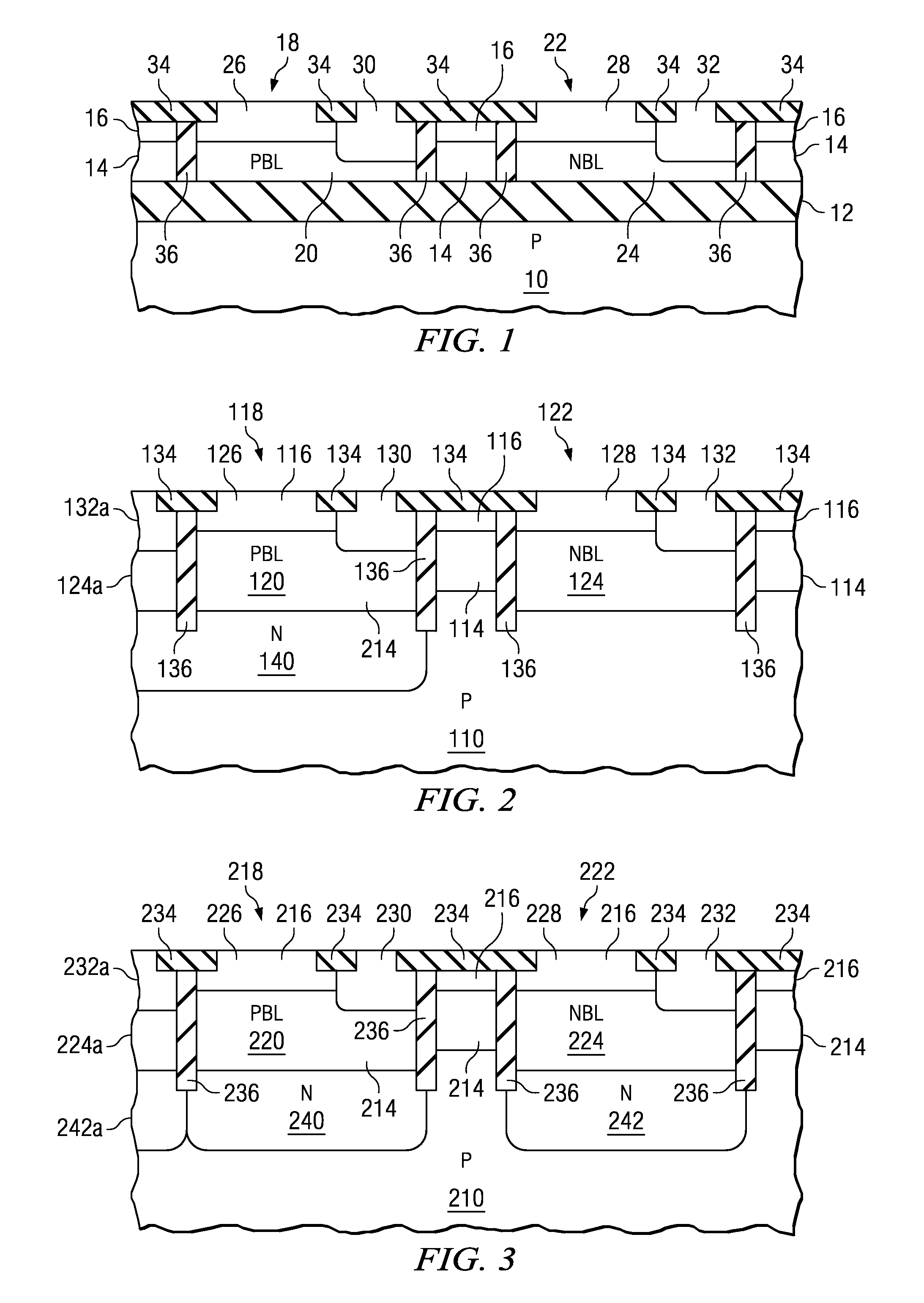
[0004]Due to many advantages associated with silicon on insulator (SOI) substrates (e.g. dielectric isolation, increased packing density, reduced cross-talk noise, latch-up immunity), high performance complementary Bipolar / BiCMOS processes often utilize SOI substrates. However, the increased cost associated with SOI substrates relative to bulk silicon wafers can be prohibitive for cost sensitive applications.
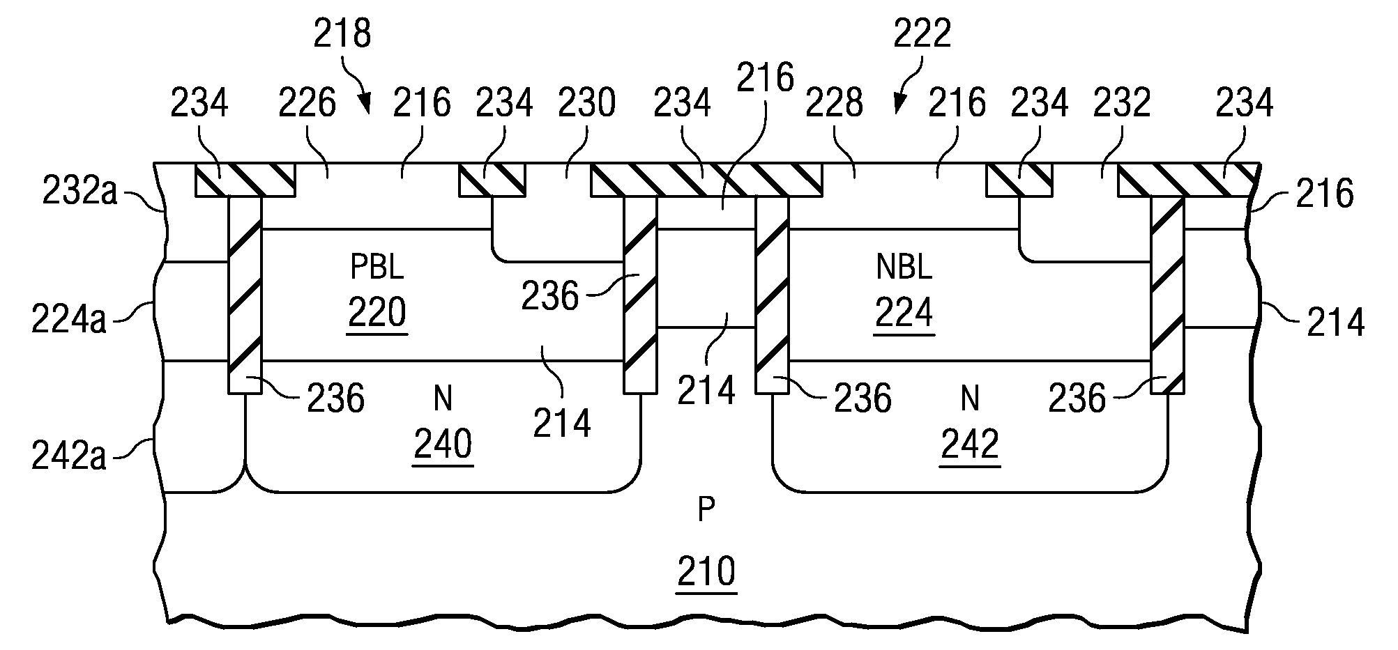
[0006]The present invention provides a method in which the bipolar transistor is junction-isolated from the substrate without requiring any additional photomasking steps, thus minimizing cost and process complexity.
[0008]The present invention further provides an integrated semiconductor structure with two complementary bipolar transistors that are built on a bulk semiconductor substrate and that are junction-isolated from the semiconductor substrate and that can be fabricated without unreasonably increasing the costs. The integrated semiconductor structure according to the present invention comprises a first bipolar transistor structure and a second complementary bipolar transistor built on a doped semiconductor substrate. The collector of the first bipolar transistor structure is of the same dopant type as the doped semiconductor substrate, and the collector of the second bipolar transistor structure is of the opposite dopant type. A doped buried region is located underneath the collector of the first transistor structure and a doped tank region of opposite dopant type is located underneath the buried region. A doped buried region is located underneath the collector of the second transistor structure and a doped tank region of same dopant type is located underneath the buried region. A contacting sinker is provided adjacent to the first transistor structure. A doped buried region is located underneath the contacting sinker. Underneath the doped buried region a doped tank region of same dopant type is provided which contacts the doped tank region of the first transistor structure.

Problems solved by technology

However, the increased cost associated with SOI substrates relative to bulk silicon wafers can be prohibitive for cost sensitive applications.
For cost sensitive applications, the added expense associated with the additional photomasking step for forming the NTANK is undesirable.

Method used


Image

  • Method for Fabricating Isolated Integrated Semiconductor Structures
  • Method for Fabricating Isolated Integrated Semiconductor Structures

Examples


Embodiment Construction

[0013]The present invention is described with reference to the attached figures, wherein like reference numerals are used throughout the figures to designate similar or equivalent elements. The figures are not drawn to scale and they are provided merely to illustrate the invention. Several aspects of the invention are described below with reference to example applications for illustration. It should be understood that numerous specific details, relationships, and methods are set forth to provide a full understanding of the invention. One skilled in the relevant art, however, will readily recognize that the invention can be practiced without one or more of the specific details or with other methods. In other instances, well-known structures or operations are not shown in detail to avoid obscuring the invention. The present invention is not limited by the illustrated ordering of acts or events, as some acts may occur in different orders and / or concurrently with other acts or events. F...


PUM


Abstract

An integrated semiconductor structure and a method for fabricating an integrated semiconductor structure in a bulk semiconductor wafer.

Description

CROSS-REFERENCE TO RELATED APPLICATIONS[0001]This application claims the benefit of priority under 35 U.S.C. 119 and 37 C.F.R. 1.55 to the prior-filed foreign application, German Application No. 10 2007 056 103.4, filed Nov. 15, 2007, titled “A Method for Fabricating Isolated Integrated Semiconductor Structures”, the entirety of which is hereby incorporated by reference.BACKGROUND OF THE INVENTION[0002]This invention relates to a method for fabricating an integrated semiconductor structure in a bulk semiconductor wafer.SUMMARY[0003]The present invention relates to a method for fabricating an integrated semiconductor structure which comprises a first bipolar transistor built on a doped semiconductor substrate, wherein the collector of the first bipolar transistor is of the same dopant type as the doped semiconductor substrate. The present invention further relates to an integrated semiconductor structure which comprises a first bipolar transistor and a second bipolar transistor built...

Claims


Application Information

Patent Timeline
IPC IPC(8): H01L21/265H01L27/06
CPCH01L21/82285H01L21/8249H01L27/1203H01L27/0623H01L27/0826H01L21/84
Inventor BALSTER, SCOTTEL-KAREH, BADIHYASUDA, HIROSHI
Owner TEXAS INSTR INC
Learn More