Unlock instant, AI-driven research and patent intelligence for your innovation.

Camera Module and Array Camera Module with Circuit Board Unit and Photosensitive Unit and Manufacturing Method Thereof

a technology of circuit board unit and camera module, which is applied in the field of single and/or array camera module with circuit board unit and photosensitive unit, can solve the problems of increasing the defective rate restricting the development similar adverse effects of the camera module, so as to reduce the overall dimension of the encapsulation portion and reduce the height of the camera module. , the effect of reducing the back focal length

Active Publication Date: 2017-09-21
NINGBO SUNNY OPOTECH CO LTD
View PDF2 Cites 8 Cited by
  • Summary
  • Abstract
  • Description
  • Claims
  • Application Information

AI Technical Summary

Benefits of technology

[0029]An object of the present invention is to provide a camera module and array camera module with circuit board unit and photosensitive unit and manufacturing method thereof, wherein the sensor of the photosensitive unit has a photosensitive portion and a non-photosensitive portion. The non-photosensitive portion of the sensor is molded by the encapsulation portion to reduce the size of the photosensitive unit and the assembled camera module.
[0074]According to a preferred embodiment of the present invention, the photosensitive sensor of the camera module includes a photosensitive area and a non-photosensitive area, wherein the non-photosensitive area is positioned around the periphery of the photosensitive area. The conjoined encapsulation portion is molded to extend to the non-photosensitive area of the photosensitive sensor so as to expand the molding area of the conjoined encapsulation portion inwardly to reduce the overall dimension of the conjoined encapsulation portion.

Problems solved by technology

According to the conventional COB technology, there are disadvantages in the assembling and coordination relationships among the circuit board 1P, the circuit components 7P, and the lens holder 3P, which also restrict the development for the camera module to become lighter and thinner.
Therefore, the assembling process of the sensor 2P, like the circuit components 7P, has the similar adverse effects to the camera module.
Besides, because the circuit components 7P and the sensor 2P are connected and provided in a common space, those dusts and pollutants can easily and adversely affect the sensor 2P that can result in undesirable occurrences such as dark spots of the assembled camera module, which increases the defective rate of the camera module.
Therefore, to mount the lens holder 3P on the circuit board 1P, a safe distance is required to be reserved between the lens holder 3P and the circuit components 7P in both horizontal direction and upward direction, that results in increasing the thickness of the camera module and the difficulty to the thickness reduction of the camera model.
Nevertheless, this adjustment space requirement will not only further increase the thickness of the camera module, rendering it substantially being more difficult to reduce the thickness of the camera module, but also cause tilt discrepancy of the assembling more easily during such multiple adhering process.
As a result, the size of the electronic device becomes larger and larger, the assemble difficulty thereof increases accordingly, and the overall size of the camera module becomes bigger and bigger.
However, the camera module installed in the current mobile electronic devices is usually a single lens camera module that can no longer satisfy the user's multi-functional application demand of the mobile electronic device in both image quality and effects of photography.
As a consequence, the consistency of the parameters, such as the dimensions and positions between the frames of the twin-lens camera modules, is poor.
Nonetheless, the circuit board 10P is usually a PCB, printed circuit board, which is relatively soft and easy to be distorted, that it is difficult to ensure the overall rigidity of the conventional twin-lens camera module.
In addition, during the usage after the twin-lens camera module is assembled, such independent structure can easily cause high positioning tolerance and instability of the relative dimensions among the elements, such as the motor-camera lens units 31P, of the imaging module 30P.
Moreover, other problems, like the photosensitive axis of the imaging module 30P easily deviating from the designated position, may easily happen.
Once any of these situation occurs, the image quality of the twin-lens camera module will be adversely affected.
For example, there are uncontrolled factors or bigger adverse impacts to the final imaging effect of the image synthesis.
As a result, these protruding circuit components 11P and gold wires 121P also cause certain disadvantageous factors to the assembling of the camera module.
Besides, because the circuit components 11P and the sensors 12P are disposed in a common space, the dusts and pollutants can easily affect the sensors 12P and such influences can result in undesirable occurrences such as dark spots of the assembled camera module that decreases the product yield rate.
Besides, comparing to the single-lens camera module, the multi-lens camera module relates to issues of coordination between multiple camera modules.
However, the consistency of the photosensitive axes of multiple camera lens modules based on the traditional COB technology is hard to be ensured.
Furthermore, the overall size of a conventional multi-lens camera module is larger, which is more sensitive to the strength and smoothness of the circuit board and, therefore, the circuit board is thicker.

Method used


Image

  • Camera Module and Array Camera Module with Circuit Board Unit and Photosensitive Unit and Manufacturing Method Thereof
  • Camera Module and Array Camera Module with Circuit Board Unit and Photosensitive Unit and Manufacturing Method Thereof
  • Camera Module and Array Camera Module with Circuit Board Unit and Photosensitive Unit and Manufacturing Method Thereof

Examples


second embodiment

[0182]It is worth mentioning that the electrical connection of the motor unit 40 is described as electrical connecting the motor unit 40 by the lead element 131 according to the above second embodiment of the present invention, but in other embodiments of the present invention, it is possible to apply different motor connecting structures 13 to connect the motor unit 40. For example, the various methods as shown in FIGS. 11A, 11B, and 11C. In other words, the various motor connecting structures as illustrated in FIGS. 11A, 11B, and 11C can be coupled with different photosensitive units respectively to provide different ways to electrically connect the motor unit. Therefore, person skilled in the art should understand that what are shown in the appended drawings shall not limit the scope of the present invention.

[0183]Referring to FIGS. 12 and 13, a photosensitive unit and a camera module thereof according to a third preferred embodiment of the present invention are illustrated. The ...

fourth embodiment

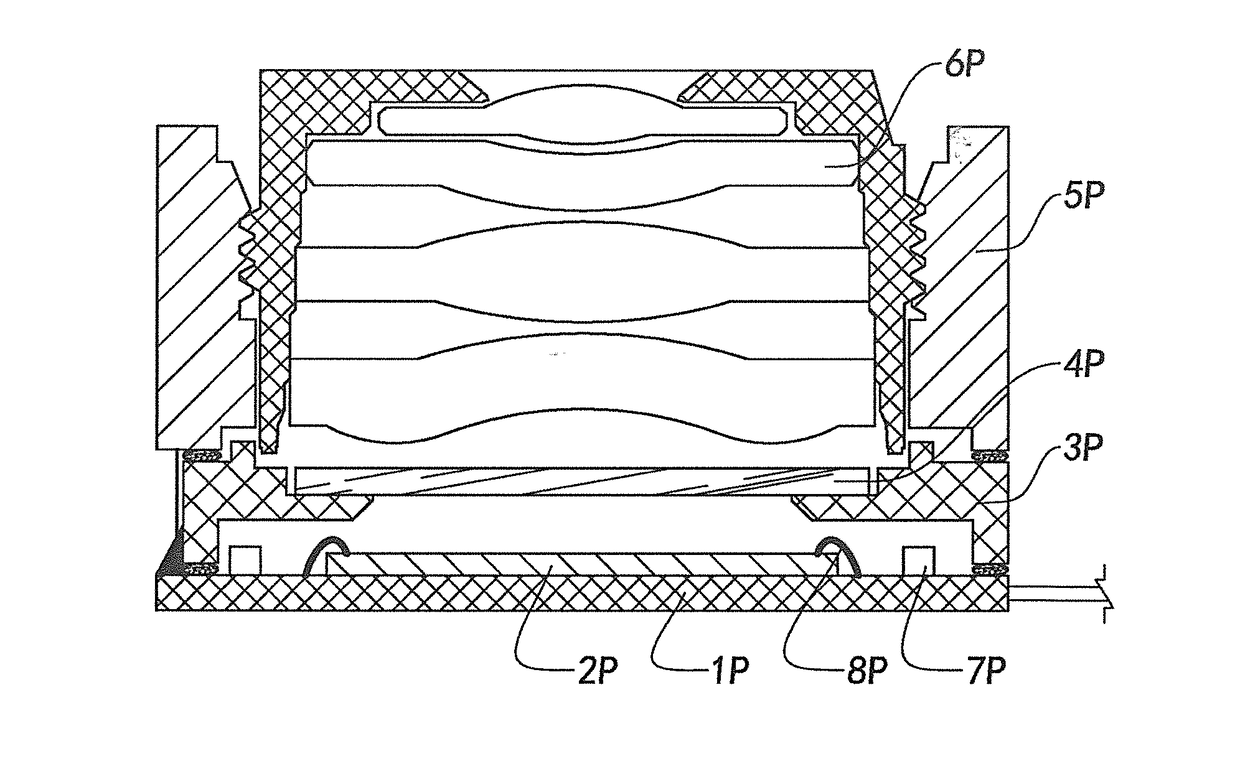
[0212]In the present fourth embodiment of the present invention, the encapsulation portion 11B is protruded to surround the outside of the photosensitive area 1211B of the photosensitive sensor 121B. Particularly, the encapsulation portion 11B integrally seal its connection, so as to provide a great sealingness and tightness. Therefore, when the photosensitive unit 10B is used to assemble the camera module, the photosensitive sensor 121B will be sealed inside the camera module to forms a sealed inner space.

[0213]In particular, the production of the photosensitive unit 10B may utilize a conventional circuit board as the main circuit board 122B. The photosensitive sensor 121B is deployed on the main circuit board 122B and electrically connected by the connecting element 124B. Then, the initially assembled main circuit board 122B and photosensitive sensor 121B are molded by, for example, injection molding machine. By means of the insert molding technique, the circuit board that has bee...

fifth embodiment

[0230]The photosensitive portion 12C includes a main circuit board 122C and a photosensitive sensor 121C, wherein the photosensitive sensor 121C is disposed on the main circuit board 122C. According to the present fifth embodiment of the present invention, the photosensitive sensor 121C is molded to connect to the main circuit board 122C.

[0231]According to the present fifth embodiment of the present invention, the photosensitive portion 12C includes a connecting circuit (not shown in the figures) and at least a circuit element 123C. The connecting circuit is preinstalled in the main circuit board 122C. The circuit element 123C is electrically connected to the connecting circuit and the photosensitive sensor 121C, wherein the photosensitive sensor 121C is arranged to perform the photosensing process thereof. The circuit element 123C is protrudingly deployed on the main circuit board 122C. The circuit element 123C can be, for example but not limited to, resistors, capacitors, diodes, ...


PUM


Abstract

A camera module and array camera module with circuit board unit and photosensitive unit and manufacturing method thereof is provided. The array camera module comprises two or more camera lenses and a circuit unit. The circuit unit comprises a circuit board portion for electrically connecting two or more photosensitive sensors of the array camera module, and a conjoined encapsulation portion integrally encapsulated on the circuit board portion. The camera lenses are respectively arranged along the photosensitive paths of the photosensitive sensors.

Description

CROSS REFERENCE OF RELATED APPLICATION[0001]This application is a Continuation application that claims the benefit of priority under 35 U.S.C. §119 to a non-provisional application, application Ser. No. 15 / 075,192, filed Mar. 20, 2016, which is incorporated herewith by reference in its entity.NOTICE OF COPYRIGHT[0002]A portion of the disclosure of this patent document contains material which is subject to copyright protection. The copyright owner has no objection to any reproduction by anyone of the patent disclosure, as it appears in the United States Patent and Trademark Office patent files or records, but otherwise reserves all copyright rights whatsoever.BACKGROUND OF THE PRESENT INVENTION[0003]Field of Invention[0004]The present invention relates to the field of camera module, and more particularly to a single and / or array camera module with circuit board unit and photosensitive unit and the manufacturing method thereof.[0005]Description of Related Arts[0006]COB (Chip On Board,...

Claims


Application Information

Patent Timeline
Patent Type & Authority Applications(United States)
IPC IPC(8): H04N5/225H01L27/146
CPCH04N5/2257H04N5/2252H04N5/2253H01L27/1469H01L27/14618H01L27/14636H01L27/14634H04N5/2254H04N13/239H01L2224/48091H04N2213/001H04N23/45H04N23/57H04N23/55H04N23/54H01L2924/00014H04N23/51
Inventor WANG, MINGZHUZHAO, BOJIETANAKA, TAKEHIKOCHEN, FEIFANMEI, QIMINDING, LIANGJIANG, HENG
Owner NINGBO SUNNY OPOTECH CO LTD