Organic el display device and method of manufacturing an organic el display device

a display device and organic el technology, applied in the direction of basic electric elements, semiconductor devices, electrical equipment, etc., can solve the problems of display defects, increase of power consumption, and possible decrease of luminance, and achieve the effect of display defects

Inactive Publication Date: 2017-10-05
JAPAN DISPLAY INC
View PDF6 Cites 1 Cited by
  • Summary
  • Abstract
  • Description
  • Claims
  • Application Information

AI Technical Summary

Benefits of technology

[0008]As in Japanese Unexamined Patent Application Publication No. 2014-44439, in the configuration where the LDD region and the heavily doped region are adjacent to each other, in the case where a position of a

Problems solved by technology

As in Japanese Unexamined Patent Application Publication No. 2014-44439, in the configuration where the LDD region and the heavily doped region are adjacent to each other, in the case where a position of a border between the LDD region and the heavily doped region is varied pixe

Method used


Image

  • Organic el display device and method of manufacturing an organic el display device
  • Organic el display device and method of manufacturing an organic el display device
  • Organic el display device and method of manufacturing an organic el display device

Examples


Embodiment Construction

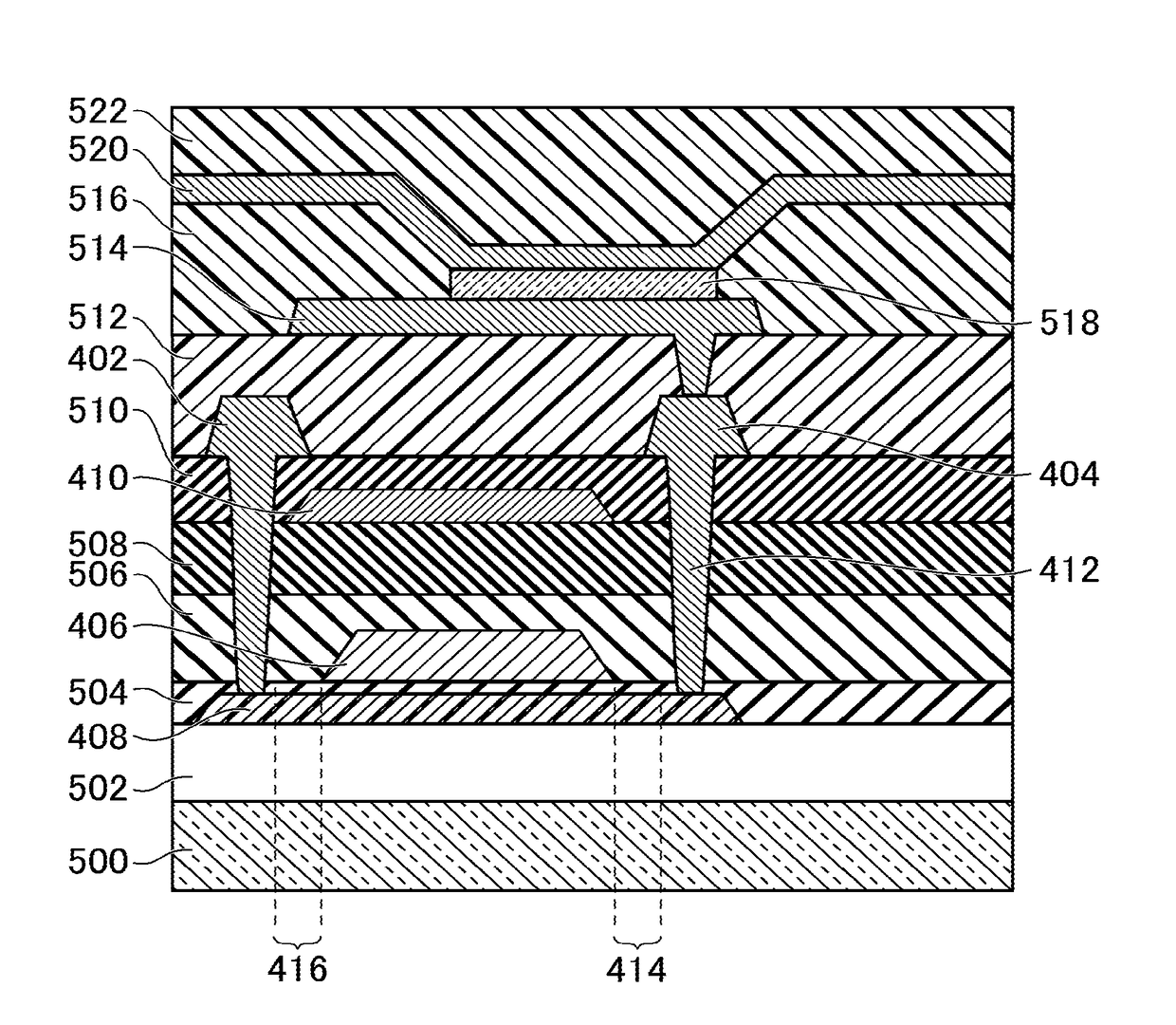
[0023]Below, respective embodiments of the present invention are explained with reference to the accompanying drawings. The disclosed embodiments are merely examples, and appropriate variations within the spirit of the present invention that can be easily arrived at by those skilled in the art are naturally included in the scope of the present invention. Further, while the width, thickness, shape, and the like of each part in the drawings may be illustrated schematically as compared with the actual embodiments in order to clarify the explanation, these are merely examples and an interpretation of the present invention should not be limited thereto. Furthermore, in the specification and respective drawings, the same reference symbols may be applied to elements similar to those that have already been illustrated in another drawing and a detailed explanation of such elements may be omitted as appropriate.

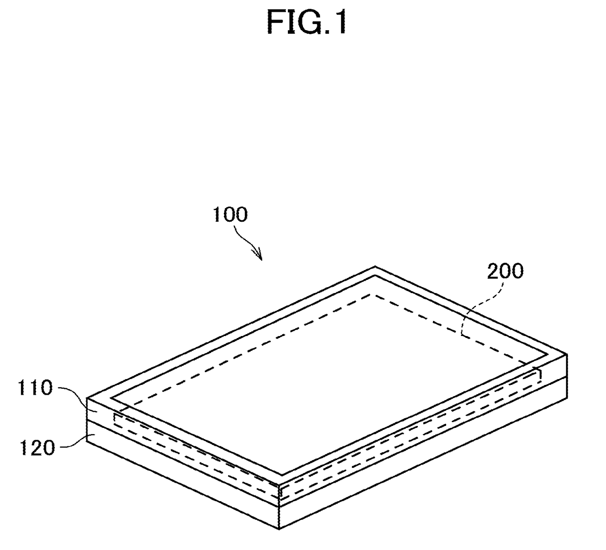
[0024]FIG. 1 is a view schematically illustrating an organic EL display device 100...


PUM


Abstract

An organic EL display device includes a plurality of pixels and a transistor in each of the pixels. The transistor includes a drain electrode and a source electrode. A first gate electrode formed between the source electrode and the drain electrode, and a semiconductor film formed at a lower layer side of the first gate electrode. A first region that is one of a region between the first gate electrode and the drain electrode and a region between the first gate electrode and the source electrode of the semiconductor film has a high density of n-type ions and a second region that is the other one of the region between the first gate electrode and the drain electrode and the region between the first gate electrode and the source electrode of the semiconductor film has a low density of n-type ions.

Description

CROSS-REFERENCE TO RELATED APPLICATION[0001]The present application claims priority from the Japanese Application JP2016-75394 filed on Apr. 4, 2016, the content of which is hereby incorporated by reference into this application.BACKGROUND OF THE INVENTION1. Field of the Invention[0002]The present invention relates to an organic EL display device and a method of manufacturing an organic EL display device.2. Description of the Related Art[0003]Recent years, an organic EL display device using a light emitting element called an organic light emitting diode (OLED) (hereinafter referred to as an organic EL element) is put into a practical use. The organic EL display device controls a current that is made to flow in an organic EL element of each pixel by using a field effect transistor provided in each pixel to thereby perform an image display.[0004]The field effect transistor performs an action of amplifying a current between a source electrode and a drain electrode in accordance with a ...

Claims


Application Information

Patent Timeline
IPC IPC(8): H01L27/32H01L51/56
CPCH01L27/3262H01L27/3248H01L51/56H01L21/266H01L29/66492H01L29/66742H01L29/78621H10K59/1213H10K59/1201H10K59/12H01L29/78624H01L29/78645H01L27/1222H01L27/124H01L29/66757H01L29/78627H10K59/123H10K71/00
Inventor MARUYAMA, SATOSHI
Owner JAPAN DISPLAY INC
Why Eureka
Try Eureka