Substrate processing apparatus, nozzle base, and manufacturing method for semiconductor device

a manufacturing method and semiconductor technology, applied in the direction of coatings, chemical vapor deposition coatings, metallic material coating processes, etc., can solve the problems of high production cost and time-consuming maintenance work, and achieve the effect of improving the maintenance effect at the time of nozzle attachment and detachmen

Active Publication Date: 2018-03-29
KOKUSA ELECTRIC CO LTD
View PDF5 Cites 312 Cited by
  • Summary
  • Abstract
  • Description
  • Claims
  • Application Information

AI Technical Summary

Benefits of technology

[0003]However, in the case of devising a structure of a nozzle base, a cost for production may be expensive and an unstable state may arise at the time of nozzle installation. The present disclosure is made in view of the above-described circumstances, and directed to providing a technique that can improve maintainability during a nozzle attachment and detachment.
[0012]According to the present disclosure, maintainability at the time of nozzle attachment and detachment can be improved.

Problems solved by technology

In many cases, nozzle maintenance is carried out by accessing from an opening of the reaction tube, and it may take time to perform the maintenance work.
However, in the case of devising a structure of a nozzle base, a cost for production may be expensive and an unstable state may arise at the time of nozzle installation.

Method used


Image

  • Substrate processing apparatus, nozzle base, and manufacturing method for semiconductor device
  • Substrate processing apparatus, nozzle base, and manufacturing method for semiconductor device
  • Substrate processing apparatus, nozzle base, and manufacturing method for semiconductor device

Examples


Embodiment Construction

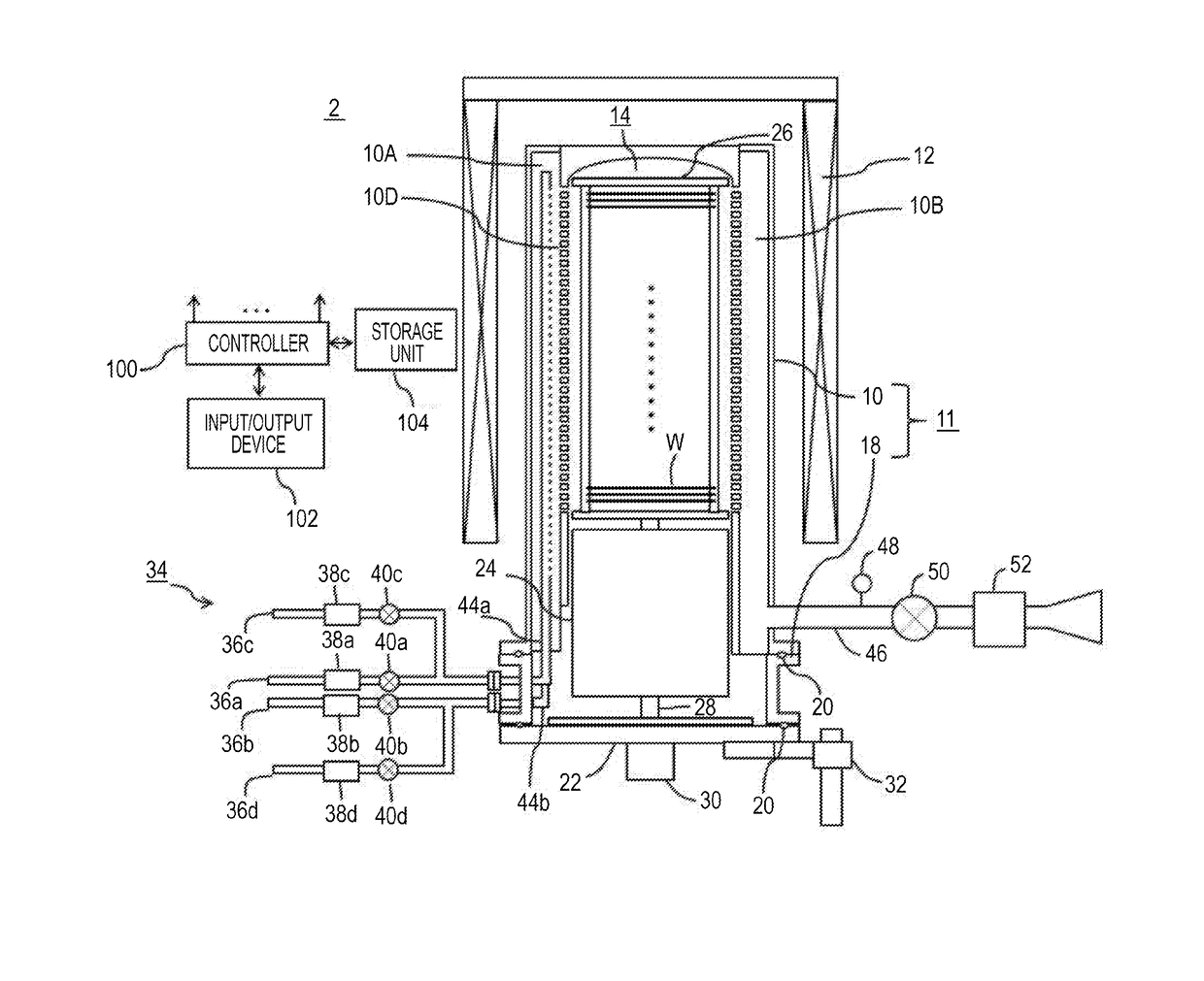
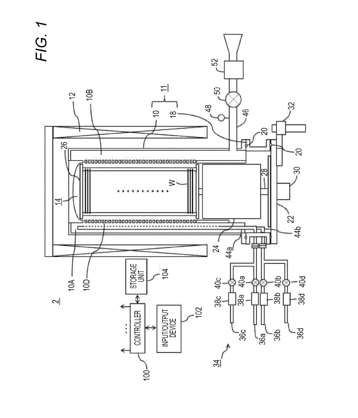
[0021]In the following, an exemplary embodiment of the present invention, not intended to be limited, will be described below with reference to the drawings. In all the drawings, note that a same or corresponding component is denoted by the same or corresponding reference sign, and redundant description will be omitted. Note that a direction toward a center of a processing container is defined as a front side (front surface side), and a direction toward outside from the center of the processing container is defined as a back side (back surface side). Additionally, note that a direction toward an upper portion of the processing container is defined as an upper side and a direction toward a lower portion of the processing container is defined as a lower side.

[0022]In the present embodiment, a substrate processing apparatus is formed as a vertical substrate processing apparatus (hereinafter referred to as processing apparatus) 2 adapted to execute a substrate processing process such as...


PUM

PropertyMeasurementUnit
widthaaaaaaaaaa
depthaaaaaaaaaa
shapeaaaaaaaaaa

Abstract

Provided is a processing container formed of a reaction tube and a manifold that supports the reaction tube from below, and adapted to process a substrate inside, a nozzle adapted to supply a processing gas to the substrate, and a connecting portion adapted to erect the nozzle inside the processing container. The connecting portion includes (1) a fixing portion formed of a cylindrical portion inserted into an introduction portion provided at the manifold, and a flange plate formed at an end portion of the cylindrical portion, and (2) a detachable portion formed of an elbow engaged with the flange plate, and an installation portion in which the nozzle is installed.

Description

BACKGROUNDTechnical Field[0001]The present invention relates to a substrate processing apparatus, a nozzle base, and a manufacturing method for a semiconductor device.Related Art[0002]In substrate processing in a manufacturing process for semiconductor devices (such as integrated circuits), for example, a vertical substrate processing apparatus that collectively processes a plurality of substrates is used. In the vertical substrate processing apparatus, a nozzle to supply a processing gas is installed inside a reaction tube by being connected and fixed to a gas introduction port provided at an inlet. In many cases, nozzle maintenance is carried out by accessing from an opening of the reaction tube, and it may take time to perform the maintenance work. Therefore, a structure of basal portion of the nozzle is devised such that the nozzle can be removed from the reaction tube to enable maintenance to be performed from inside of the reaction tube (JP 2015-185578A).SUMMARY[0003]However, ...

Claims


Application Information

Patent Timeline
Patent Type & Authority Applications(United States)
IPC IPC(8): C23C16/455H01L21/205H01L21/31
CPCC23C16/455H01L21/31H01L21/205C23C16/402C23C16/45578C23C16/45587C23C16/4584H01L21/67017H01L21/67103
Inventor YOSHIDA, HIDENARI
Owner KOKUSA ELECTRIC CO LTD
Why Eureka
Try Eureka