Waveguide-type optical element

Active Publication Date: 2018-05-03
SUMITOMO OSAKA CEMENT CO LTD
View PDF3 Cites 1 Cited by
  • Summary
  • Abstract
  • Description
  • Claims
  • Application Information

AI Technical Summary

Benefits of technology

This patent aims to provide a better understanding of a certain component in a computer network. By analyzing the data on this component, the patent seeks to improve the overall performance and reliability of the network. The technical effect of this patent is to enhance the efficiency and reliability of computer networks by studying and improving the performance of their components.

Problems solved by technology

However, the decrease in the driving voltage and the broadening of the band has a conflicting relationship, and it is difficult to broaden the band without increasing the driving voltage.
However, in actual cases, the upper limit of the thicknesses of electrodes that can be formed is approximately 50 μm, and there is a limitation in broadening the band by increasing the thicknesses of electrodes.
However, as the thickness of the resist increases, stress in the resist increases, the attaching force between the resist and the substrate decreases, and a possibility of the resist being peeled off in the middle of the formation of the electrode increases.
In addition, the time taken to form the electrodes also increases in accordance with the thickness, and productivity degrades.

Method used


Image

  • Waveguide-type optical element
  • Waveguide-type optical element
  • Waveguide-type optical element

Examples


first embodiment

[0044]First, a first embodiment of the present invention will be described.

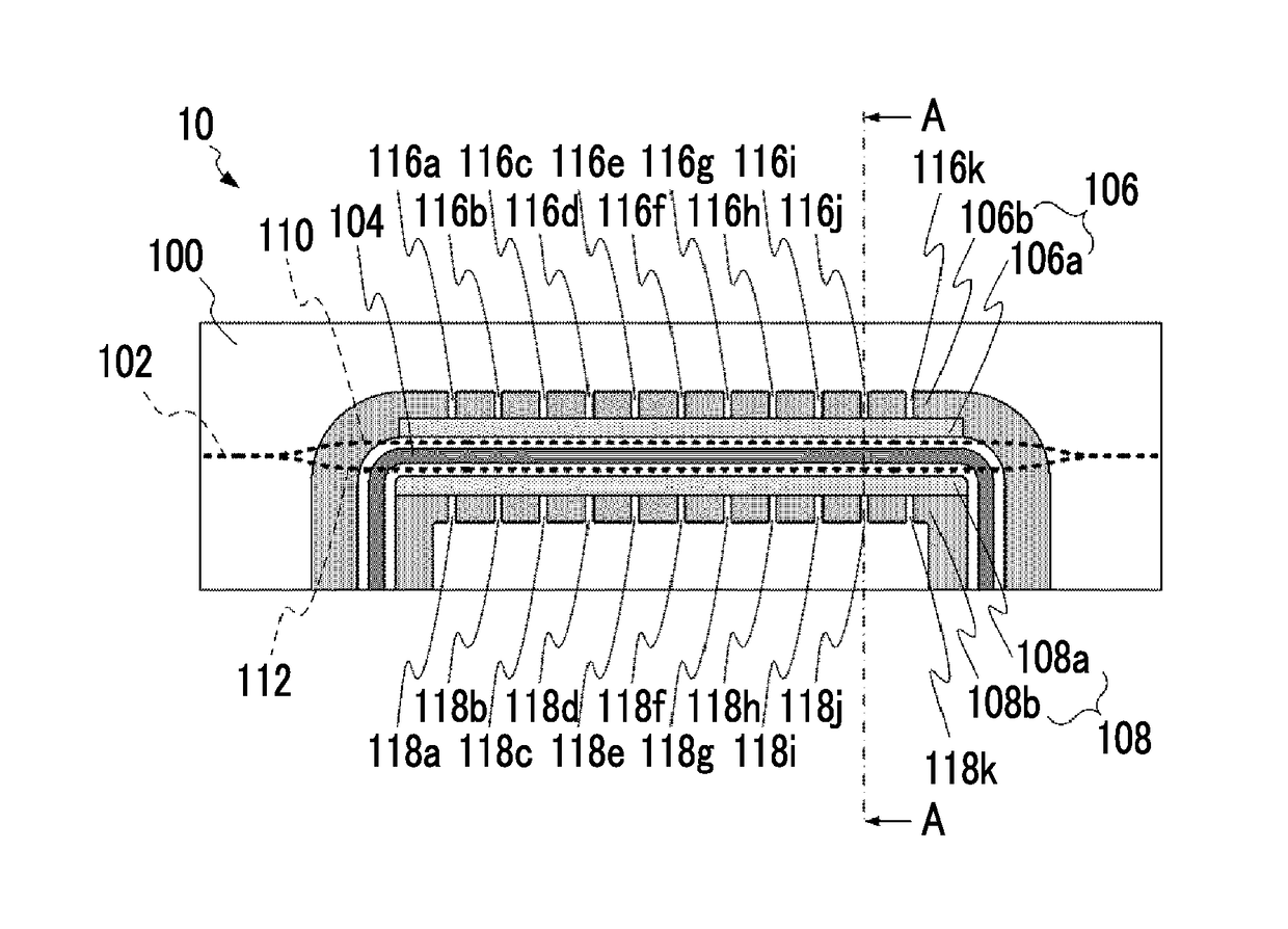
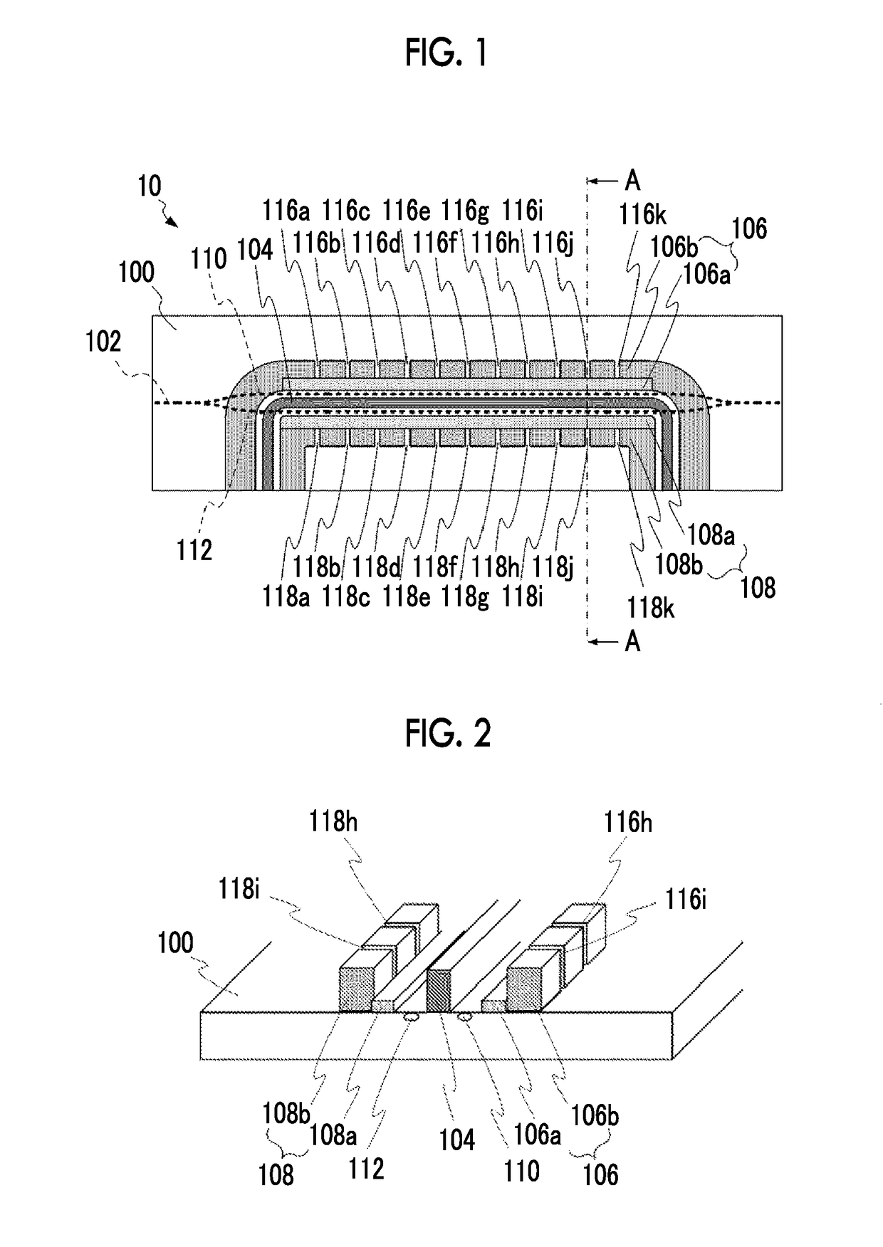
[0045]FIG. 1 is a view illustrating the constitution of a waveguide-type optical element according to the first embodiment of the present invention.

[0046]The present waveguide-type optical element 10 is a Mach-Zehnder-type optical modulator and has a Mach-Zehnder (MZ)-type optical waveguide 102 formed on a substrate 100 and a central electrode 104 and two ground electrodes 106 and 108 which constitute a CPW-type electrode.

[0047]The substrate 100 is a substrate made of lithium niobate (LN) which is an electro-optic material and is, for example, an X-cut LN substrate. The MZ-type optical waveguide 102 has parallel waveguides 110 and 112, and the central electrode 104 is formed parallel to the parallel waveguides 110 and 112 in a region on the surface of the substrate 100 which is surrounded by the parallel waveguides 110 and 112. In addition, the ground electrodes 106 and 108 are formed respectively at position...

second embodiment

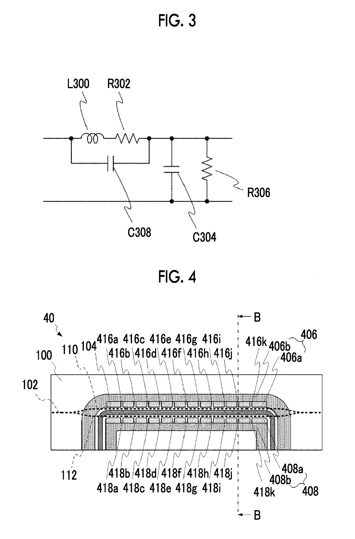
[0055]Next, a second embodiment of the present invention will be described.

[0056]FIG. 4 is a view illustrating the constitution of a waveguide-type optical element according to the second embodiment of the present invention. Meanwhile, in FIGS. 4 and 5, the same constituent elements as those in the waveguide-type optical element 10 according to the first embodiment illustrated in FIGS. 1 and 2 will be given the same reference number as in FIGS. 1 and 2, and the description thereof in the above-described waveguide-type optical element 10 according to the first embodiment will be applied to the present embodiment.

[0057]The present waveguide-type optical element 40 has the same constitution as that of the waveguide-type optical element 10 according to the first embodiment, but includes ground electrodes 406 and 408 instead of the ground electrodes 106 and 108. The ground electrodes 406 and 408 have the same constitution as that of the ground electrodes 106 and 108 except for the fact t...

third embodiment

[0062]Next, a third embodiment of the present invention will be described.

[0063]FIG. 6 is a view illustrating the constitution of a waveguide-type optical element according to the third embodiment of the present invention. Meanwhile, in FIGS. 6 and 7, the same constituent elements as those in the waveguide-type optical element 10 according to the first embodiment illustrated in FIGS. 1 and 2 will be given the same reference number as in FIGS. 1 and 2, and the description thereof in the above-described waveguide-type optical element 10 according to the first embodiment will be applied to the present embodiment.

[0064]The present waveguide-type optical element 60 has the same constitution as that of the waveguide-type optical element 10 according to the first embodiment, but includes ground electrodes 606 and 608 instead of the ground electrodes 106 and 108. The ground electrodes 606 and 608 have the same constitution as that of the ground electrodes 106 and 108. However, a difference ...


PUM


Abstract

In a waveguide-type optical element, broaderband operation becomes possible.The waveguide-type optical element includes optical waveguides (110 and 112) formed on a substrate (100) having an electro-optic effect and a control electrode for controlling an optical wave that is transmitted through the optical waveguide, the control electrode comprises a central electrode (104) and ground electrodes (106 and 108), the central electrode being formed along the optical waveguide, and the ground electrodes being formed so as to put the central electrode therebetween in a surface direction of the substrate at a predetermined distance from the central electrode, and the central electrode or the ground electrodes have multiple pairs of facets, each comprising two facets facing each other, along a transmission direction of high-frequency signals that are transmitted through the central electrode and the ground electrodes.

Description

TECHNICAL FIELD[0001]The present invention relates to a waveguide-type optical element including an optical waveguide and a control electrode for controlling an optical wave that is transmitted through the optical waveguide, and particularly to a broadband waveguide-type optical element capable of acting in a broad frequency range.BACKGROUND ART[0002]In recent years, in the field of optical communication or optical measurement, waveguide-type optical elements such as optical modulators having an optical waveguide formed on a substrate having an electro-optic effect have been frequently used. Waveguide-type optical elements, generally, include the optical waveguide and a control electrode for controlling an optical wave that is transmitted through the optical waveguide.[0003]As the above-described waveguide-type optical elements, for example, Mach-Zehnder-type optical modulators in which lithium niobate (LiNbO3) (also referred to as “LN”), which is a ferroelectric crystal, is used fo...

Claims


Application Information

Patent Timeline
IPC IPC(8): G02F1/225G02F1/035H01P3/00
CPCG02F1/2257G02F1/035H01P3/003G02F2001/212G02F1/225G02F1/2255G02F1/212
Inventor KONDOU, KATSUTOSHIICHIKAWA, JUNICHIROKATAOKA, TOSHIO
Owner SUMITOMO OSAKA CEMENT CO LTD
Why Eureka
Try Eureka