
Photoelectric conversion device, image forming apparatus, photoelectric conversion method, and non-transitory recording medium

a technology of photoelectric conversion and image forming apparatus, which is applied in the direction of color television details, television system details, television systems, etc., can solve the problems of failing to eliminate the influence of defective pixels on the image, and achieve the effect of improving the photoelectric conversion method

Active Publication Date: 2018-05-24
RICOH KK
View PDF4 Cites 24 Cited by
  • Summary
  • Abstract
  • Description
  • Claims
  • Application Information

AI Technical Summary

Benefits of technology

The patent describes an improved photoelectric conversion device with a plurality of photoelectric conversion pixels. The device includes an imaging unit that generates image data for each color based on light received by the pixels. A position identifying unit detects defective pixels that output abnormal signals and stores position information about them. An interpolation determining unit determines whether to perform an interpolation process on the defective pixels based on the pixel values of peripheral pixels. The interpolation process approximates the electrical signal of the defective pixels to a normal level. The invention also includes an improved image forming apparatus that uses this photoelectric conversion device to form images and a photoelectric conversion method for executing the device.

Problems solved by technology

If the defective pixel corresponds to an edge portion of a fine line forming a character or the like or an edge portion of a pattern, however, the interpolation process may replace the value of the defective pixel with an incorrect value, failing to eliminate the influence of the defective pixel on the image.

Method used


Image

  • Photoelectric conversion device, image forming apparatus, photoelectric conversion method, and non-transitory recording medium
  • Photoelectric conversion device, image forming apparatus, photoelectric conversion method, and non-transitory recording medium
  • Photoelectric conversion device, image forming apparatus, photoelectric conversion method, and non-transitory recording medium

Examples


first embodiment

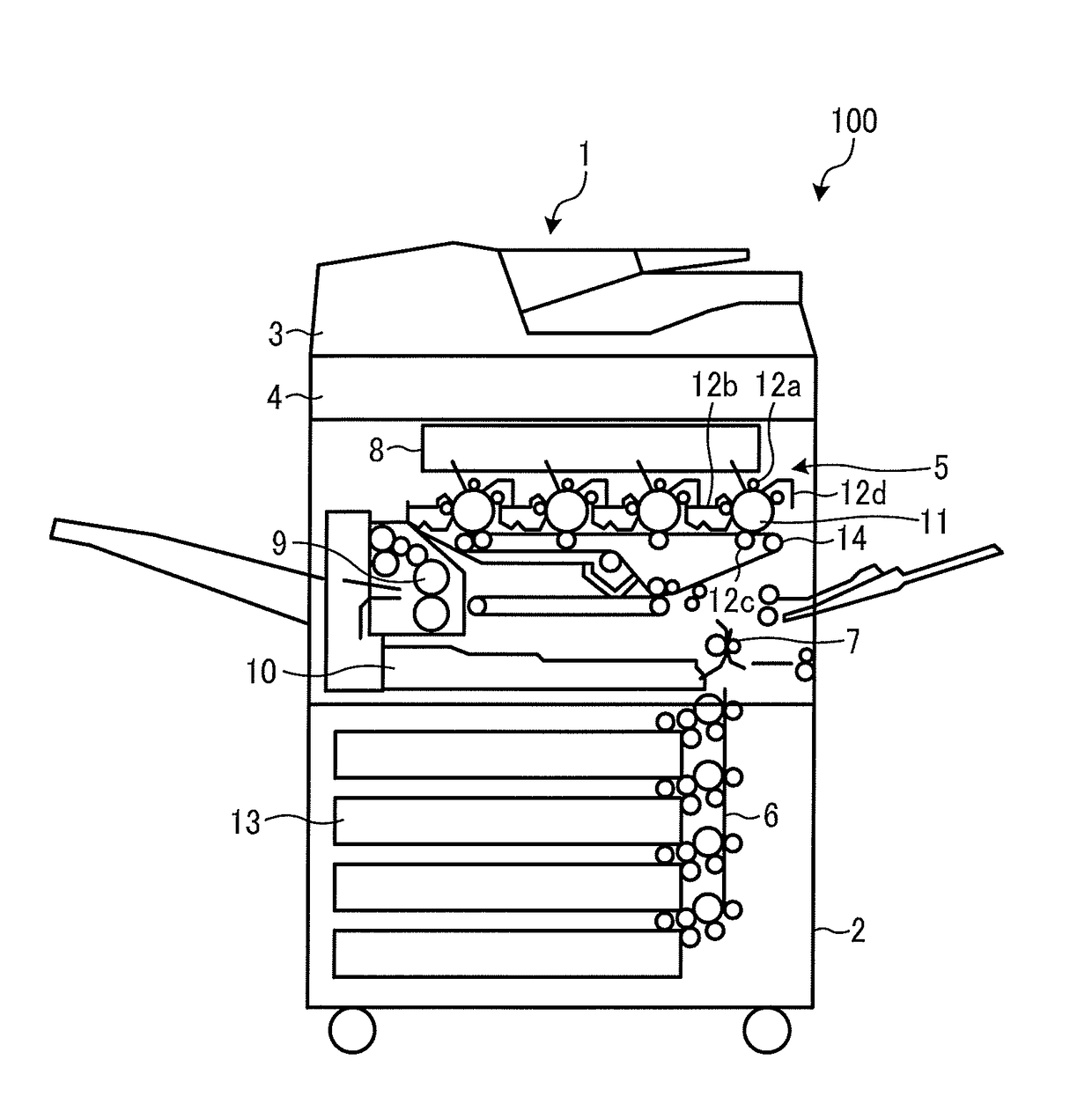
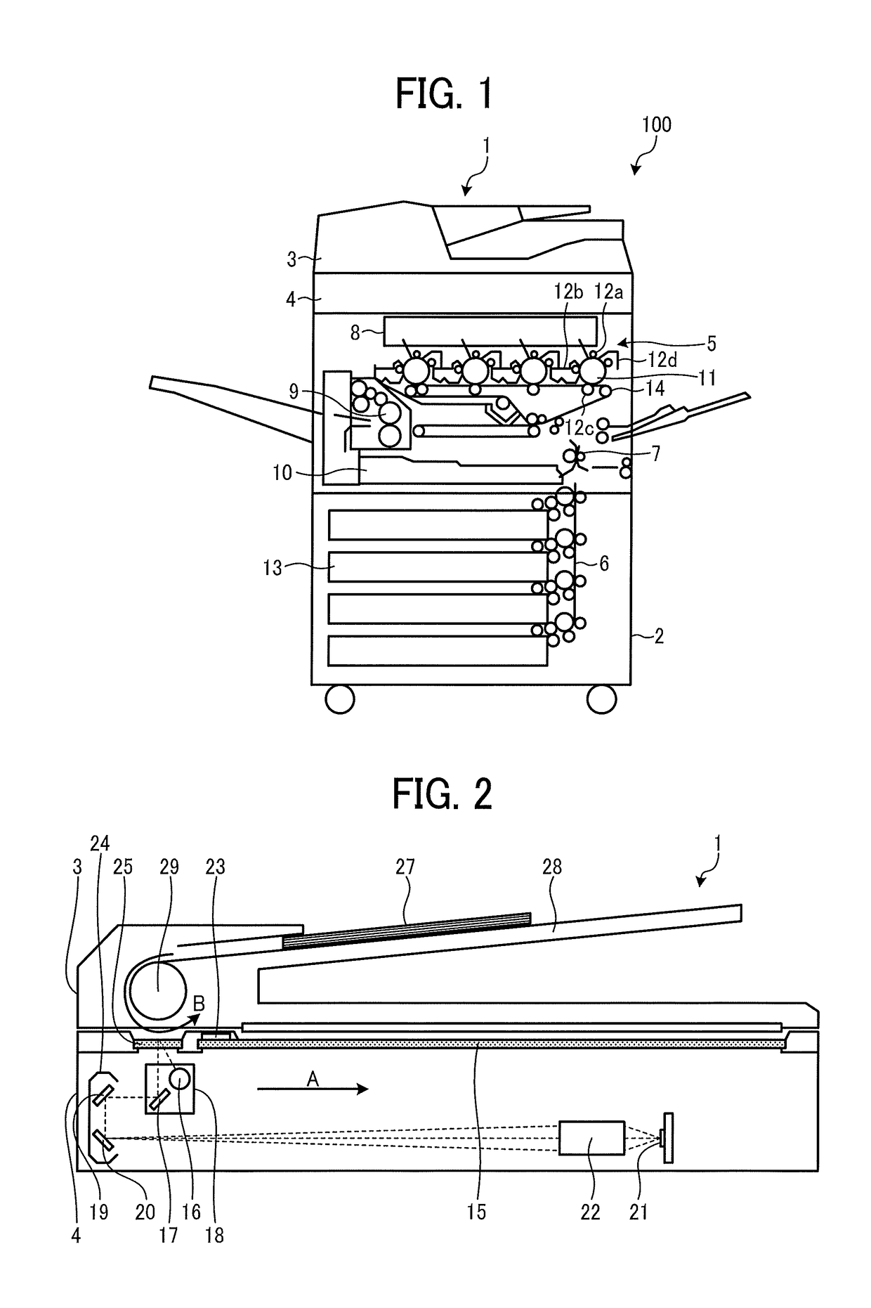
[0037]FIG. 1 illustrates the MFP 100 as viewed from a side of the MFP 100. In FIG. 1, a main body 2 of the MFP 100 is seen through. As illustrated in FIG. 1, the MFP 100 includes a reading device 1 and the main body 2. The reading device 1 includes an automatic document feeder (ADF) 3 and a scanner mechanism 4.

[0038]The main body 2 includes an image forming unit 5 employing a tandem system, registration rollers 7 that supply a recording sheet to the image forming unit 5 from one of sheet feeding units 13 via a transport path 6, an optical writing device 8, a fixing and transporting unit 9, and a duplex tray 10. The image forming unit 5 includes four photoconductor drums 11 corresponding to four colors: yellow (Y), magenta (M), cyan (C), and black (K). Each of the photoconductor drums 11 is surrounded by image forming components, such as a charger 12a, a developing device 12b, a transfer device 12c, a cleaner 12d, and a discharger. In FIG. 1, only the rightmost one of the photocondu...

second embodiment

[0097]A configuration of the MFP 100 according to the present invention will now be described.

[0098]The influence of the defective pixel on the image increases with an increase in the density of the image on one of the lateral sides of the defective pixel in a color channel corresponding to the defective pixel. For instance, if the image includes a black portion, and if an edge of the black portion is read in a defective pixel, an image area corresponding to one of the lateral sides of the defective pixel has a low density, and an image area corresponding to the other lateral side of the defective pixel has a high density, consequently making the influence of the defective pixel on the image conspicuous.

[0099]According to the second embodiment, therefore, the interpolation process is executed if the foregoing conditions for performing the interpolation are met by the difference ΔL and the mean Lave of the image data of the left peripheral pixels of the defective pixel or the differe...

third embodiment

[0105]A configuration of the MFP 100 according to the present invention will now be described.

[0106]When a yellow color patch is read, for example, high-level image data (i.e., a low-density image) is generated in the R channel and the G channel, while low-level image data (i.e., a high-density image) is generated in the B channel. In this case, if there is a defective pixel in the B channel for generating the low-level image data, the read image of the yellow color patch is formed with image data affected by the defective pixel. Consequently, the defective pixel may affect the low-density image ultimately generated from RGB images. In other words, although the influence of the defective pixel is normally inconspicuous in a yellow image having a low density, the presence of a defective pixel in the channel of a high-density color may affect the low-density image ultimately generated from the RGB images.

[0107]According to the third embodiment, therefore, the interpolation determining...


PUM


Abstract

A photoelectric conversion device having plural photoelectric conversion pixels includes an imaging unit, a position identifying unit, an interpolation determining unit, and an interpolation processing unit. The imaging unit generates image data for each of plural colors based on light received in the photoelectric conversion pixels. The position identifying unit detects in the photoelectric conversion pixels a defective pixel outputting an electrical signal at an abnormal level, and stores position information of the defective pixel. The interpolation deter mining unit determines, based on respective pixel values of peripheral pixels peripheral to the defective pixel, whether to perform an interpolation process on the defective pixel. The interpolation processing unit performs the interpolation process on the defective pixel when the interpolation determining unit determines to perform the interpolation process on the defective pixel. The interpolation process approximates the electrical signal of the defective pixel to an electrical signal at a normal level.

Description

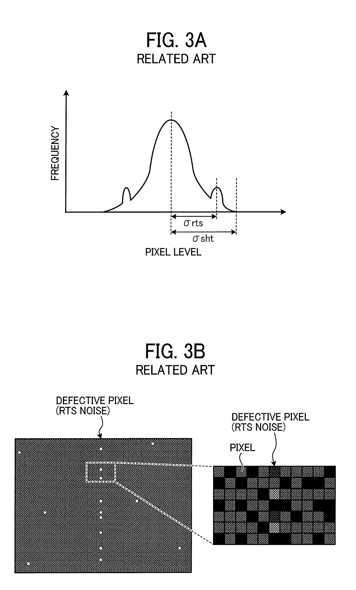
CROSS-REFERENCE TO RELATED APPLICATION[0001]This patent application is based on and claims priority pursuant to 35 U.S.C. § 119(a) to Japanese Patent Application No. 2016-228370 filed on Nov. 24, 2016, in the Japan Patent Office, the entire disclosure of which is hereby incorporated by reference herein.BACKGROUNDTechnical Field[0002]The present invention relates to a photoelectric conversion device, an image forming apparatus, a photoelectric conversion method, and a non-transitory recording medium.Description of the Related Art[0003]An interpolation process has been known in which abnormal image data generated in a defective pixel in an imaging device is interpolated with image data of pixels peripheral to the defective pixel. For example, to reduce random telegraph signal (RTS) noise in an image, an image processing device may perform the interpolation process on a target pixel if the noise amount of the target pixel exceeds the mean shot noise amount of pixels peripheral to the t...

Claims


Application Information

Patent Timeline
Patent Type & Authority Applications(United States)
IPC IPC(8): H04N5/367H04N5/217
CPCH04N5/367H04N5/2173H04N2201/04787H04N1/409H04N1/58H04N1/401H04N23/81H04N25/68H04N23/84H04N25/60
Inventor SHIRADO, HIROKINAKAZAWA, MASAMOTOYABUUCHI, MASAYUKI
Owner RICOH KK
Learn More