Photoelectric conversion device, photoelectric conversion method, and image forming apparatus

a photoelectric conversion and conversion method technology, applied in the direction of electrical devices, diodes, radiation controlled devices, etc., can solve the problems of increase the adverse effect of rts noise, so as to improve the photoelectric conversion method

Active Publication Date: 2018-06-21
RICOH KK
View PDF22 Cites 18 Cited by
  • Summary
  • Abstract
  • Description
  • Claims
  • Application Information

AI Technical Summary

Benefits of technology

[0004]In one aspect of this disclosure, there is provided an improved photoelectric conversion device including a generation circuit and a controller. The generation circuit generates an image signal according to an intensity of light being input. The controller to control the generation circuit to generate a dark-time image signal equivalent to an image signal generated by the generation circuit without exposure to external light.
[0005]In another aspect of this disclosure there is provided an improved photoelectric conversion method including generating an image signal according to an intensity of light received by a generation circuit; and controlling the generation circuit to generate a dark-time image signal equivalent to an image signal generated by the generation circuit without exposure to external light.
[0006]In still another aspect of this disclosure there is provided an improved image forming apparatus including a document tray to place a document; a light source to emit light to the document; and a photoelectric conversion device to receive the light reflected by the document. The photoelectric conversion device includes a generation circuit and a controller. The generation circuit generates an image signal according to an intensity of the light received. The controller controls the generation circuit to generate a dark-time image signal equivalent to an image signal generated h the generation circuit without exposure to light coming from an outside of the image forming apparatus.

Problems solved by technology

The occurrence of the RTS noise adversely produces a defective image.
Such an adverse effect of the RTS noise becomes more noticeable with the development of miniaturization of the CMOS sensors.

Method used


Image

  • Photoelectric conversion device, photoelectric conversion method, and image forming apparatus
  • Photoelectric conversion device, photoelectric conversion method, and image forming apparatus
  • Photoelectric conversion device, photoelectric conversion method, and image forming apparatus

Examples


first embodiment

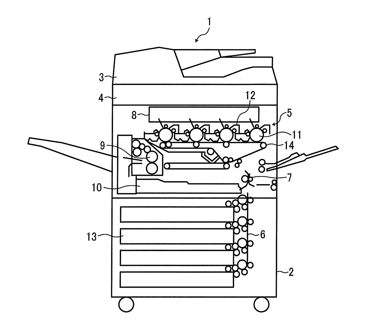
[0082]The MFP according to the first embodiment includes a noise detector 71, a memory 72, and a pixel corrector 73 disposed at the subsequent stage of the photoelectric conversion element 56 as illustrated in FIG. 13. The noise detector 71 detects a physical address of a pixel (the pixel-signal generation circuit 61 for a pixel) that generates noise in the photoelectric conversion element 56. The memory 72 stores address data regarding the pixel from which noise has been detected. The pixel corrector 73 performs correction processing on the pixel from which noise has been detected.

[0083]Note that some or all of the photoelectric conversion element 56, the noise detector 71, the memory 72, and the pixel corrector 73 are integrated as a single circuit. In the example of FIG. 13, the photoelectric conversion element 56, the noise detector 71, the memory 72, and the pixel corrector 73 are sealed in a package to be apparently a large-scale integration circuit (LSI), that is, formed as a...

second embodiment

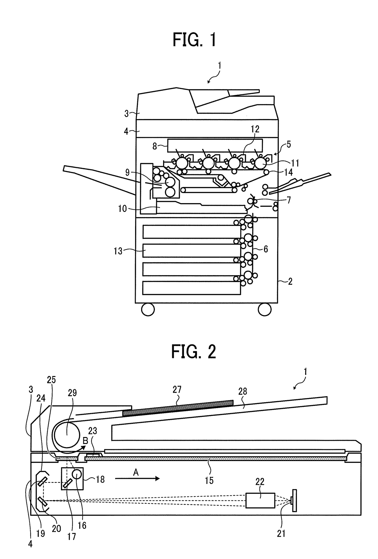
[0093]Next, a description is given of a MFP according to the second embodiment. The above-described pseudo light shielding mode is a mode to output a reset electrical potential and obtain data (dark-time image signal) that is equivalent to the image signal of dark-time data obtained with light shielded. The MFP according to the second embodiment obtains such a dark-time image signal in the following manner.

[0094]FIG. 17 illustrates timing charts of signals of the components (see FIG. 6) of the photoelectric conversion element 56 in the MFP according to the second embodiment in the pseudo light shielding mode. Same as FIG. 15, FIG. 17(a) is a timing chart of a line synchronous signal (Lsync) for one line. FIG. 17(b) is a timing chart of a switch control signal (SL) to on-off control the switch SL. FIG. 17(c) is a timing chart of a reset signal (RT) to on-off control the reset switch RT to reset the electrical potential in the floating diffusion FD to a rest electrical potential AVDD_...

third embodiment

[0097]Hereinafter, a description is given of a MFP according to a third embodiment of the present disclosure. FIG. 18 illustrates timing charts of signals of the components (see FIG. 6) of the photoelectric conversion element 56 in the MFP according to the third embodiment in the pseudo light shielding mode. Same as FIG. 17, FIG. 18(a) is a timing chart of a line synchronous signal (Lsync) for one line. FIG. 18(b) is a timing chart of a switch control signal (SL) to on-off control the switch SL. FIG. 18(c) is a timing chart of a reset signal (RT) to on-off control the reset switch RT to reset the electrical potential in the floating diffusion FD to a rest electrical potential AVDD_RT. FIG. 18(d) is a timing chart of a transfer control signal (TX) to on-off control the charge-transfer switch TX to transfer charges accumulated in the photodiode PD to the floating diffusion FD. FIG. 18(e) is an illustration of the timing and level of the image signal (Pix_out) output from the pixel-sig...


PUM


Abstract

A photoelectric conversion device includes a generation circuit and a controller. The generation circuit generates an image signal according to an intensity of light being input. The controller controls the generation circuit to generate a dark-time image signal equivalent to an image signal generated by the generation circuit without exposure to external light.

Description

CROSS-REFERENCE TO RELATED APPLICATION[0001]This patent application is based on and claims priority pursuant to 35 U.S.C. § 119(a) to Japanese Patent Application No. 2016-246959, filed on Dec. 20, 2016 in the Japan Patent Office, the entire disclosure of which is hereby incorporated by reference herein.BACKGROUNDTechnical Field[0002]Embodiments of the present disclosure relate to a photoelectric conversion device, a photoelectric conversion method, and an image forming apparatus.Background Art[0003]One of noise generated by a complementary metal oxide semiconductor (CMOS) image sensor is known as a random telegraph signal (RTS) noise that randomly occurs in a specific pixel. The occurrence of the RTS noise adversely produces a defective image. Such an adverse effect of the RTS noise becomes more noticeable with the development of miniaturization of the CMOS sensors.SUMMARY[0004]In one aspect of this disclosure, there is provided an improved photoelectric conversion device including ...

Claims


Application Information

Patent Timeline
Patent Type & Authority Applications(United States)
IPC IPC(8): H01L27/146H04N1/12H04N1/40
CPCH01L27/14643H04N1/126H04N1/40056H04N1/1906
Inventor INOUE, KEITANAKAZAWA, MASAMOTOSHIRADO, HIROKI
Owner RICOH KK
Why Eureka
Try Eureka