
Method and apparatus for repairing memory device

Active Publication Date: 2018-06-28
SK HYNIX INC +1
View PDF0 Cites 7 Cited by
  • Summary
  • Abstract
  • Description
  • Claims
  • Application Information

AI Technical Summary

Benefits of technology

The present patent enables high-speed searching for a repair solution in a multi-block memory that has various spare memories, leading to higher repair efficiency.

Problems solved by technology

However, such high integration density may increase the probability of an occurrence of defective memory cells, and the increase of the defective memory cells may lower a memory yield of fabricating semiconductor memories.
However, because a multi-block memory includes various spare memories applied thereto, a repair speed in the multi-block memory is rapidly increased, and the test cost is increased.

Method used


Image

  • Method and apparatus for repairing memory device
  • Method and apparatus for repairing memory device
  • Method and apparatus for repairing memory device

Examples


Embodiment Construction

[0014]Various embodiments will be described below in more detail with reference to the accompanying drawings such that this disclosure will be thorough and complete, and will fully convey the scope of the present disclosure to those skilled in the art. Throughout the disclosure, like reference numerals refer to like parts throughout the various figures and embodiments of the present disclosure.

[0015]Moreover, detailed descriptions related to publicly known functions or configurations will be ruled out in order not to unnecessarily obscure subject matters of the present disclosure.

[0016]The terms such as first and second may be used to describe various components, but the components are not limited by the terms, and the terms are used to distinguish one component from another component.

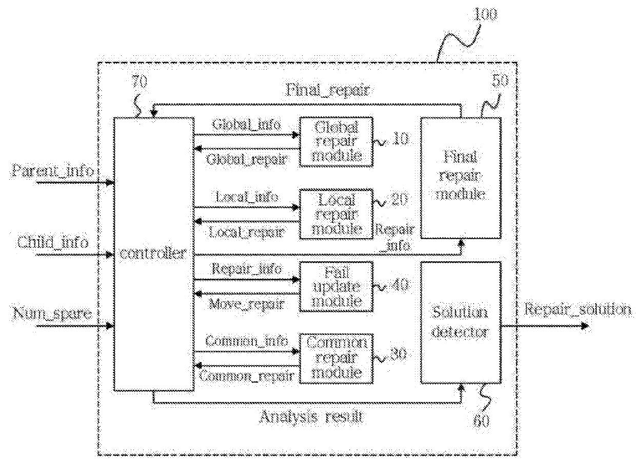
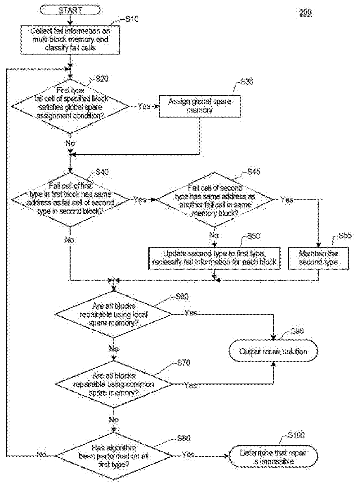
[0017]FIG. 1 is a block diagram illustrating an apparatus (hereinafter, referred to as a memory repair apparatus) 100 for repairing a memory device according to an embodiment.

[0018]Referring to FIG. 1,...


PUM


Abstract

A method of repairing a memory device may include collecting fail information on fail cells in a multi-block memory, classifying the fail cells into first and second types, and repairing the fail cells in the multi-block memory using one or more of a global spare memory, a local spare memory, and a common spare memory, based on the fail information.

Description

CROSS-REFERENCE TO RELATED APPLICATION[0001]The present application claims priority of Korean Patent Application No. 10-2016-0179308, filed on Dec. 26, 2016, which is incorporated herein by reference in its entirety.BACKGROUND1. Field[0002]Embodiments of the present disclosure relate to a semiconductor memory, and more particularly, to a method and an apparatus for repairing a semiconductor memory.2. Description of the Related Art[0003]Recently, development of semiconductor process technology has significantly increased the integration density of a semiconductor memory. However, such high integration density may increase the probability of an occurrence of defective memory cells, and the increase of the defective memory cells may lower a memory yield of fabricating semiconductor memories.[0004]In order to improve the memory yield, a fail test process and a repair solution search process for memory cells may be performed. The repair solution search process may have a repair speed var...

Claims


Application Information

Patent Timeline
IPC IPC(8): G11C29/44G11C29/00
CPCG11C29/44G11C29/838G11C29/80G11C29/72G11C2029/4402G11C29/4401G11C29/04G11C29/808
Inventor KANG, SUNG HOKIM, JOO YOUNGCHO, KEE WONLEE, HA YOUNGKIM, SANG DOOJUN, HONGSHINKIM, WOONG HEE
Owner SK HYNIX INC
Features
  • Generate Ideas
  • Intellectual Property
  • Life Sciences
  • Materials
  • Tech Scout
  • Unparalleled Data Quality
  • Higher Quality Content
  • 60% Fewer Hallucinations
Learn More