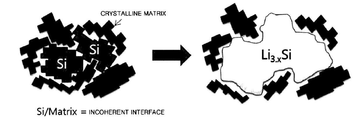
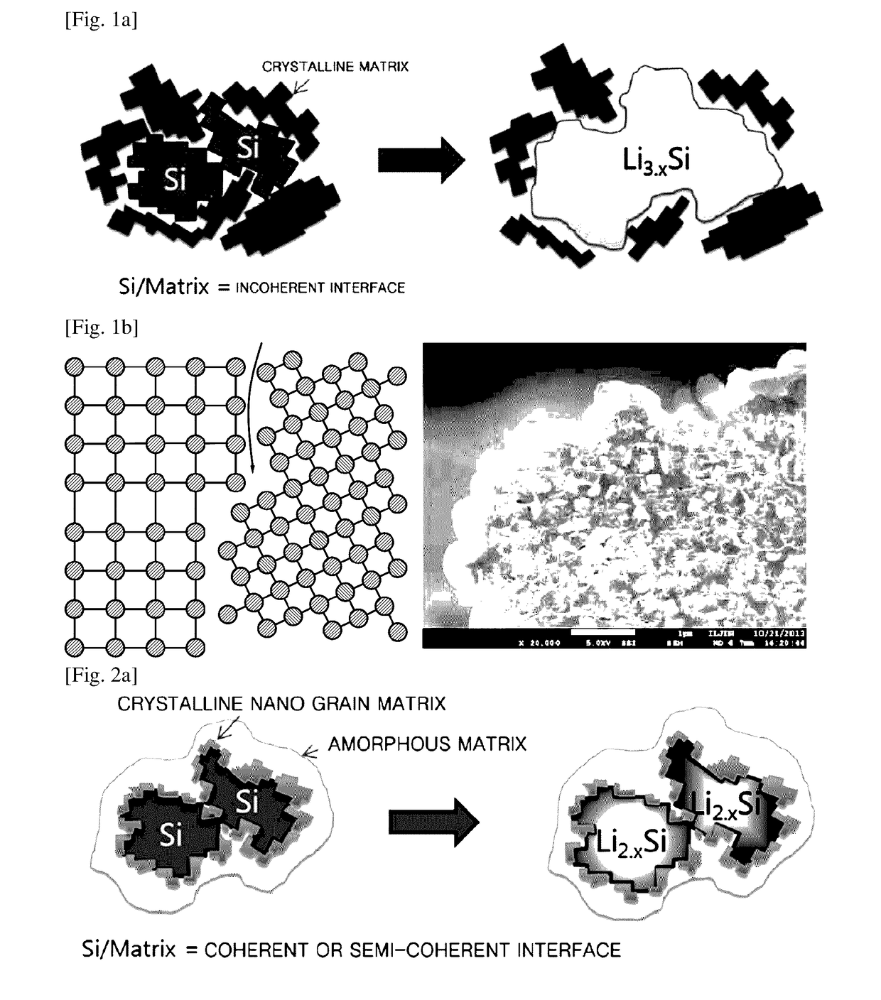
Negative electrode active material for secondary battery and secondary battery including the same
- Summary
- Abstract
- Description
- Claims
- Application Information
AI Technical Summary
Benefits of technology
Problems solved by technology
Method used
Image

Examples
experimental example 3
tive Electrode Active Material of Si70Ti15Fe15
[0146]In the meantime, Experimental Example 3 is a negative electrode active material about Si70Ti15Fe15, and the present negative electrode active material does not have a cubic structure and has a crystalline structure. Accordingly, a dispersal is considerably generated after 50 cycles. The reason is determined that a crystal structure of the matrix is different and the matrix itself exhibits a crystalline property.
[0147]FIG. 9A is a diagram illustrating an XRD peak characteristic and a state before a life test of a negative electrode active material of Experimental Example 3, and FIG. 9B is a diagram illustrating a state where a discharge capacity is considerably decreased due to a dispersal phenomenon after 50 cycles.
[0148]According to the XRD peak characteristic illustrated in FIG. 9A, it is shown that TiFeSi2 that is the matrix phase is crystalline, and in FIG. 9B, it is shown well that a discharge capacity is decreased from 1,100 ...
experimental example 4
tive Electrode Active Material of Si60(Cu20Al80)30Fe5Ti5
[0149]Experimental Example 4 is a negative electrode active material of Si60(Cu20Al80)30Fe5Ti5, and in the present negative electrode active material, the matrix is amorphous according to the XRD characteristic. However, it is exhibited that a life characteristic is relatively excellent, but a dispersal phenomenon after 50 cycles is also incurred. The reason is that a crystal structure and a lattice parameter of the matrix are considerably different from those of the silicon crystal.
[0150]FIG. 10A is a diagram illustrating an XRD peak characteristic and a state before a life test of the negative electrode active material, and illustrates states at the time of the slow cooling and the fast cooling. In the meantime, FIG. 10B illustrates a SEM picture of a cross-section of an electrode plate, in which a side reaction layer material is filled in the interface while the interface between silicon and a matrix is separated after 50 cy...
experimental example 5
tive Electrode Active Material of Si60(Cu20Al80)32.5Fe5Zr2.5
[0151]In the meantime, Experimental Example 5 is a negative electrode active material of Si60(Cu20Al80)32.5Fe5Zr2.5, and in the present negative electrode active material, the matrix is amorphous according to the XRD characteristic. However, it is exhibited that a life characteristic is relatively excellent, but a dispersal phenomenon after 50 cycles is also incurred. The reason is that a crystal structure and a lattice parameter of the matrix are considerably different from those of the silicon crystal.
[0152]FIG. 11A is a diagram illustrating an XRD peak characteristic and a state before a life test of the negative electrode active material, and illustrates states at the time of the slow cooling and the fast cooling. In the meantime, FIG. 11B illustrates a state in which the matrix material is dispersed, expansion is severe, and a capacity is sharply decrease after 50 cycles.
PUM
 Abstract
Description
Claims
Application Information
 - R&D Engineer
- R&D Manager
- IP Professional
- Industry Leading Data Capabilities
- Powerful AI technology
- Patent DNA Extraction
Browse by: Latest US Patents, China's latest patents, Technical Efficacy Thesaurus, Application Domain, Technology Topic.
© 2024 PatSnap. All rights reserved.Legal|Privacy policy|Modern Slavery Act Transparency Statement|Sitemap