

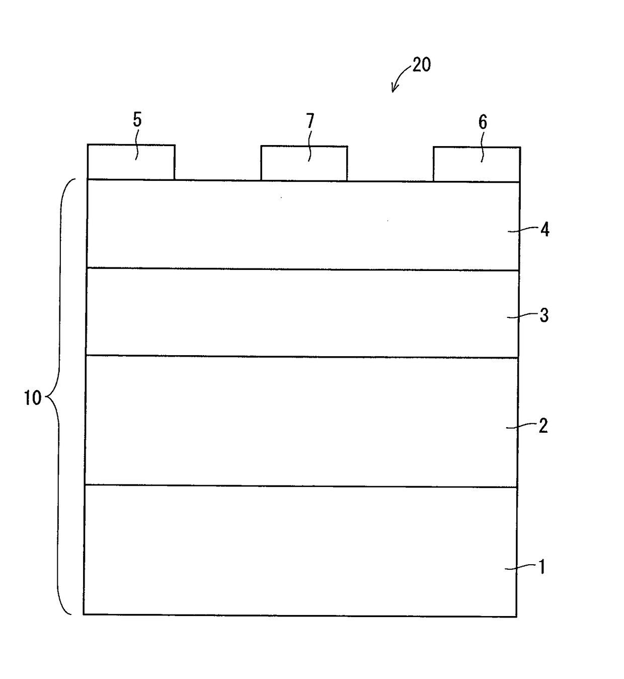
Epitaxial substrate for semiconductor elements, semiconductor element, and manufacturing method for epitaxial substrates for semiconductor elements
- Summary
- Abstract
- Description
- Claims
- Application Information
AI Technical Summary
Benefits of technology
Problems solved by technology
Method used
Image

Examples
Example
Example 1
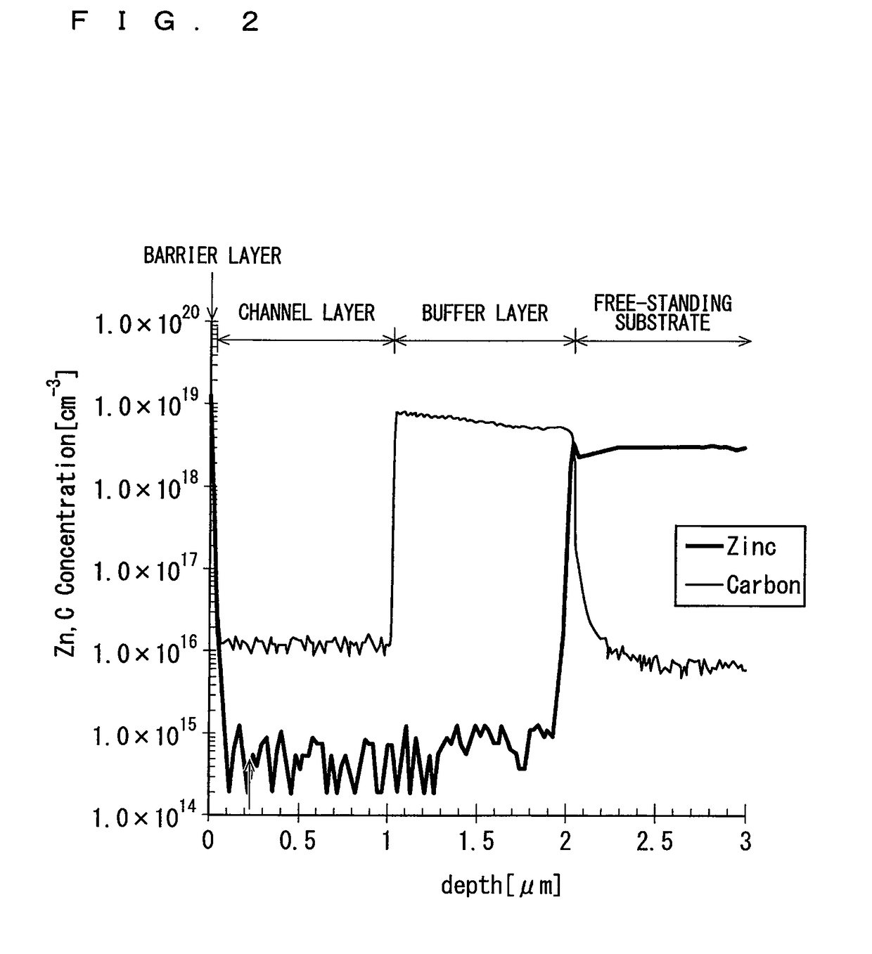
[0099](Manufacture of Zn-Doped GaN Single Crystal Substrate by Flux Method)
[0100]A GaN low-temperature buffer layer is formed to have a thickness of 30 nm at a temperature of 550° C. on a surface of a c-plane sapphire substrate having a diameter of 2 inches and a thickness of 0.43 mm, and subsequently, a GaN thin film having a thickness of 3 μm is formed by the MOCVD method at a temperature of 1050° C., thereby obtaining a MOCVD-GaN template usable as a seed substrate.
[0101]A Zn-doped GaN single crystal layer is formed by the Na flux method using the MOCVD-GaN template which has been obtained as the seed substrate.
[0102]Specifically, the MOCVD-GaN template was firstly disposed in an alumina crucible, and subsequently, the alumina crucible was filled with 30 g of metal Ga, 45 g of metal Na, 1 g of metal Zn, and 100 mg of C. The alumina crucible was put in a heating furnace and heated for approximately 100 hours with a furnace temperature of 850° C. and a furnace pressure of ...
Example
Comparative Example 1
[0144]The HEMT element was manufactured under the condition similar to that of the Example 1 except that the growth condition of the GaN buffer layer was as follows, differing from the Example 1. The condition for forming the GaN buffer layer is a condition that it is confirmed in advance that an amount of doped C is small compared with the Example 1.
[0145]GaN buffer layer:
[0146]Formation temperature=1050° C.;
[0147]Reactor pressure=30 kPa;
[0148]Gas ratio of group 15 to group 13=500;
[0149]Thickness=300 nm.
[0150]The SIMS measurement was performed on the HEMT element, which had been obtained, in the manner similar to the Example 1, and each concentration of the Zn element and the C element in the epitaxial substrate was examined.
[0151]FIG. 4 is a drawing illustrating a concentration profile of the Zn element and the C element in the epitaxial substrate according to the present Comparative Example. FIG. 5 is an enlarged view in a neighborhood of an interface between...
Example
Examples 2 to 6, Comparative Examples 2 to 5
[0157]The HEMT elements were manufactured under the conditions similar to that of the Example 1 except that growth conditions of the GaN buffer layer (the growth temperature, the reactor pressure, the gas ratio of group 15 to group 13, and the formation thickness), for example, were variously changed. Then, a distribution in the depth direction of the Zn concentration and the C concentration in the HEMT element, which had been obtained, was obtained by the SIMS measurement, and the value R was calculated.
[0158]A list of a result thereof is shown by Table 1 together with the results of the Example 1 and the Comparative Example 1.
TABLE 1SIMS measurementZn concentrationGrowth condition of GaN buffer layerfrom barrierGaslayer / channelratio ofClayer interfaceGrowthReactorgroup 15CollapseconcentrationLogarithm change ratio ofin downwardtemperaturepressuretoThicknessevaluationin GaN bufferZn concentrationdirection by[° C.][kPa]group 13[nm]Value Rl...
PUM
| Property | Measurement | Unit |
|---|---|---|
| Carrier concentration | aaaaa | aaaaa |
| Carrier concentration | aaaaa | aaaaa |
| Temperature | aaaaa | aaaaa |
Abstract
Description
Claims
Application Information