Epitaxial substrate for semiconductor elements, semiconductor element, and manufacturing method for epitaxial substrates for semiconductor elements

Active Publication Date: 2018-08-30
NGK INSULATORS LTD
View PDF1 Cites 0 Cited by
  • Summary
  • Abstract
  • Description
  • Claims
  • Application Information

AI Technical Summary

Benefits of technology

The present invention relates to a method of manufacturing an epitaxial substrate for semiconductor elements. The method includes steps of preparing a semi-insulating free-standing substrate, forming a buffer layer, forming a channel layer, and forming a barrier layer. The buffer layer is formed as a diffusion suppressing layer to prevent diffusion of Zn from the free-standing substrate into the channel layer, resulting in a reduction of current collapse in the semiconductor element. This patent aims to provide an epitaxial substrate that suppresses current collapse.

Problems solved by technology

However, there arises a problem that large numbers of defects occurs in a GaN film which is heteroepitaxially grown on the different material substrates due to a difference of lattice constant and heat expansion coefficient between GaN and the different material substrates.

Method used


Image

  • Epitaxial substrate for semiconductor elements, semiconductor element, and manufacturing method for epitaxial substrates for semiconductor elements
  • Epitaxial substrate for semiconductor elements, semiconductor element, and manufacturing method for epitaxial substrates for semiconductor elements
  • Epitaxial substrate for semiconductor elements, semiconductor element, and manufacturing method for epitaxial substrates for semiconductor elements

Examples


experimental example 1

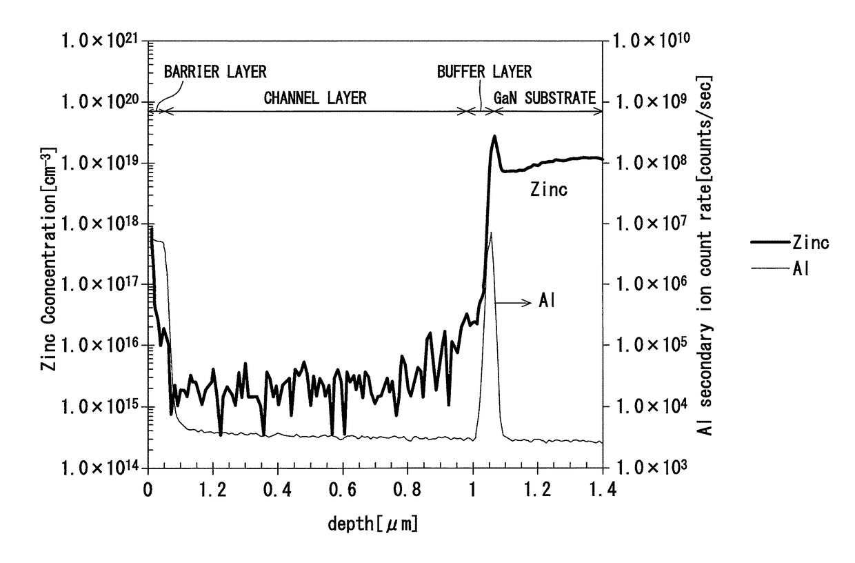
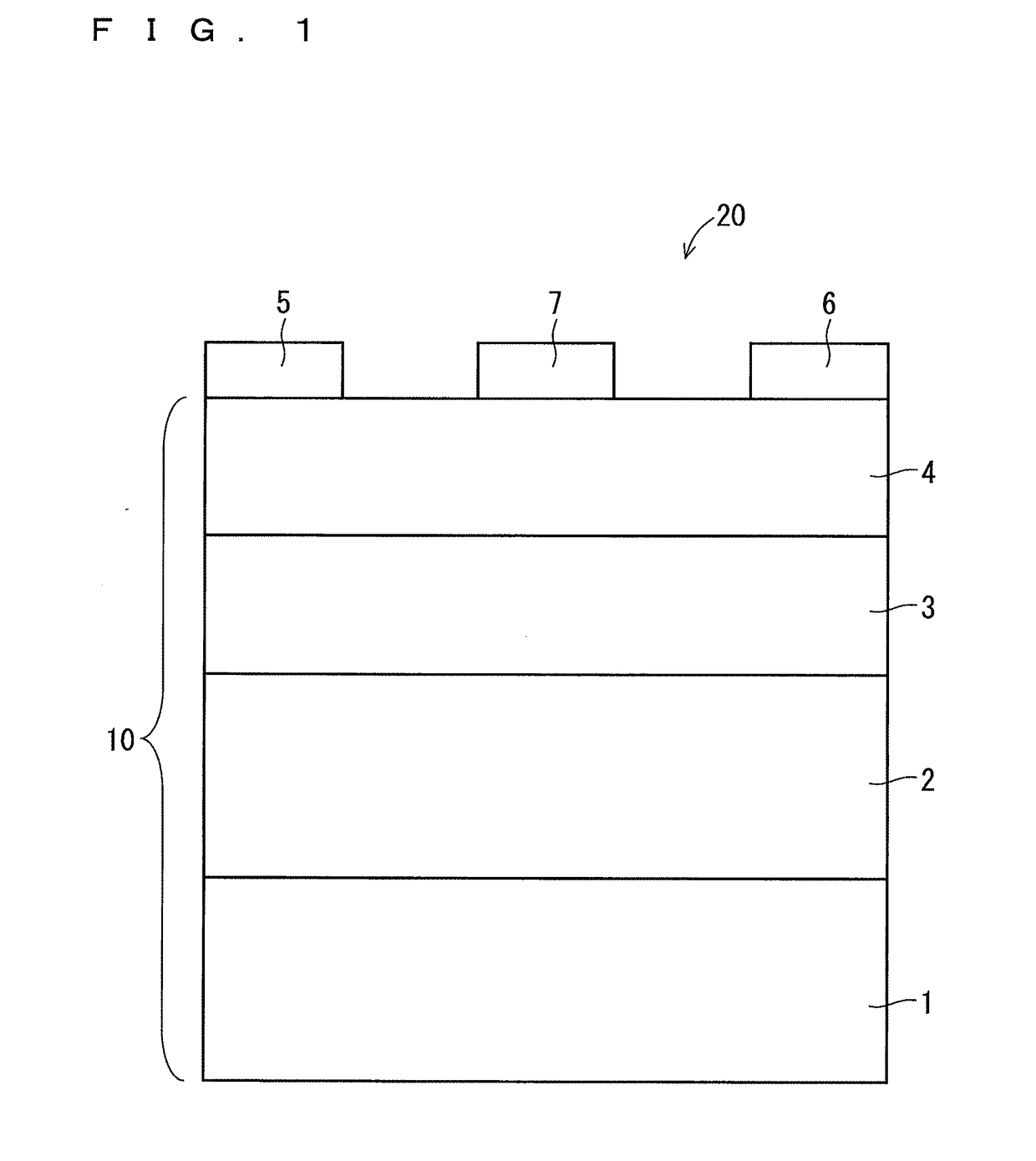
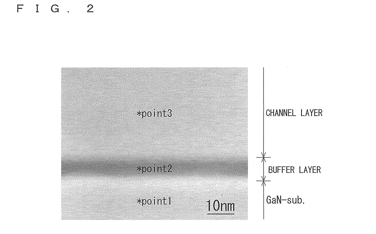
[0097]After the Zn-doped GaN single crystal free-standing substrate was manufactured, seven types of epitaxial substrates were manufactured, using the free-standing substrate as a base substrate, under the same condition except that a thickness of the buffer layer was varied. Furthermore, the HEMT element was manufactured using each epitaxial substrate. In the following, common Samples No. 1-1 to No. 1-7 are used for the seven types of epitaxial substrates and the HEMT elements manufactured using each of the epitaxial substrates.

[0098](Manufacture of Zn-Doped GaN Single Crystal Substrate by Flux Method)

[0099]A GaN low-temperature buffer layer is formed to have a thickness of 30 nm at a temperature of 550° C. on a surface of a c-plane sapphire substrate having a diameter of 2 inches and a thickness of 0.43 mm, and subsequently, a GaN thin film having a thickness of 3 μm is formed by the MOCVD method at a temperature of 1050° C., thereby obtaining a MOCVD-GaN template usable as a seed...

experimental example 2

[0159]After the Zn-doped GaN single crystal free-standing substrate was manufactured under the conditions of manufacture and the procedures similar to those in the Experimental Example 1, four types of epitaxial substrates were manufactured using the free-standing substrate as a base substrate. The conditions of manufacture in the above case were the same as that in the Experimental Example 1 except that the gas ratio of Al source gas to group 13 source gas in the formation of the AlGaN buffer layer was varied to vary the Al molar ratio p in the buffer layer. More specifically, the gas ratio of Al source gas to group 13 source gas in the formation of the buffer layer was varied at four levels of 1.0, 0.9, 0.7, and 0.5. A thickness of the buffer layer was set to 10 nm.

[0160]Since the conditions of manufacture of the Zn-doped GaN substrate are the same as that in the Experimental Example 1, a dislocation density thereof is estimated to be substantially the same as Sample No. 1-4.

[0161...

experimental example 3

[0167]After the Zn-doped GaN single crystal free-standing substrate was manufactured by the procedures similar to those in the Experimental Example 1, three types of epitaxial substrates were manufactured using the free-standing substrate as a base substrate, and the HEMT elements were manufactured using each epitaxial substrate.

[0168]However, in manufacturing each Zn-doped GaN single crystal free-standing substrate, a growth time was varied in forming the GaN single crystal layer by the flux method so that the thickness of the GaN single crystal layer formed on the surface of the MOCVD-GaN template was varied. This is intended to obtain the Zn-doped GaN single crystal free-standing substrates having the different dislocation densities. More specifically, the thickness of the GaN single crystal layer was varied at three levels of 1000 pm, 600 pm, and 200 pm by varying a heat-holding time of keeping a heating temperature at 850° C. to three levels of 100 hours, 70 hours, and 40 hours...


PUM

PropertyMeasurementUnit
Temperatureaaaaaaaaaa

Abstract

Provided is an epitaxial substrate for semiconductor elements which suppresses an occurrence of current collapse. The epitaxial substrate for the semiconductor elements includes: a semi-insulating free-standing substrate formed of GaN being doped with Zn; a buffer layer being adjacent to the free-standing substrate; a channel layer being adjacent to the buffer layer; and a barrier layer being provided on an opposite side of the buffer layer with the channel layer therebetween, wherein the buffer layer is a diffusion suppressing layer formed of AlpGa1-pN (0.7≤p≤1) and suppresses diffusion of Zn from the free-standing substrate into the channel layer.

Description

CROSS-REFERENCE TO RELATED APPLICATIONS[0001]This is a continuation of International Application No. PCT / JP2016 / 082367, filed Nov. 1, 2016, which claims the benefit of U.S. Provisional Application No. 62 / 249,565, filed Nov. 2, 2015, Japanese Application No. 2016-005164, filed Jan. 14, 2016 and PCT / JP2016 / 079619, filed Oct. 5, 2016, all of which are hereby incorporated by reference herein in their entirety.TECHNICAL FIELD[0002]The present invention relates to a semiconductor element, and particularly to a semiconductor element constituted by using a free-standing substrate that is made of semi-insulating GaN.BACKGROUND ART[0003]Nitride semiconductors, which have direct-transition-type wide band gap, high breakdown electric field, and high saturation electron velocity, have been used as light emission devices such as LED or LD and semiconductor materials for high-frequency / high-power electronic devices.[0004]Typical structures of the nitride electronic devices include high electron mo...

Claims


Application Information

Patent Timeline
IPC IPC(8): H01L21/205C23C16/34H01L29/778H01L29/812H01L29/66H01L21/02H01L29/40
CPCH01L21/205C23C16/34H01L29/778H01L29/812H01L29/66007H01L21/0254H01L29/401H01L21/02458H01L21/0262H01L29/7786H01L29/2003H01L29/201H01L29/207C23C16/303H01L21/02389H01L21/0251H01L21/02293H01L21/28017H01L2924/1033H01L2924/10344C30B19/02C30B29/406H01L29/205H01L29/66462H01L29/7787
Inventor ICHIMURA, MIKIYAMAEHARA, SOTAKURAOKA, YOSHITAKA
Owner NGK INSULATORS LTD
Why Eureka
Try Eureka