Semiconductor device

Active Publication Date: 2013-11-21
FUJI ELECTRIC CO LTD
View PDF15 Cites 2 Cited by
  • Summary
  • Abstract
  • Description
  • Claims
  • Application Information

AI Technical Summary

Benefits of technology

The invention provides a semiconductor device that can have a high resistance to reverse recovery, while keeping costs low. This is achieved by increasing the resistance of the peripheral portion of a p type diffusion region in contact with a metal electrode through an insulating film. Additionally, the inner circumferential end of the insulating film is shaped in a non-straight-line shape to further decrease the concentration of reverse recovery current. Overall, this configuration allows for effective suppression of reverse recovery current with minimal extra cost.

Problems solved by technology

If a resistant amount of the FWD with respect to the high voltage and high current, that is, a reverse recovery resistant amount is low, element breakdown easily occurs at a site where the reverse recovery current is concentrated.
In general, it is considered to be very difficult that the insulating film 109 having no defects is formed in the wafer process.

Method used


Image

  • Semiconductor device
  • Semiconductor device
  • Semiconductor device

Examples


first embodiment

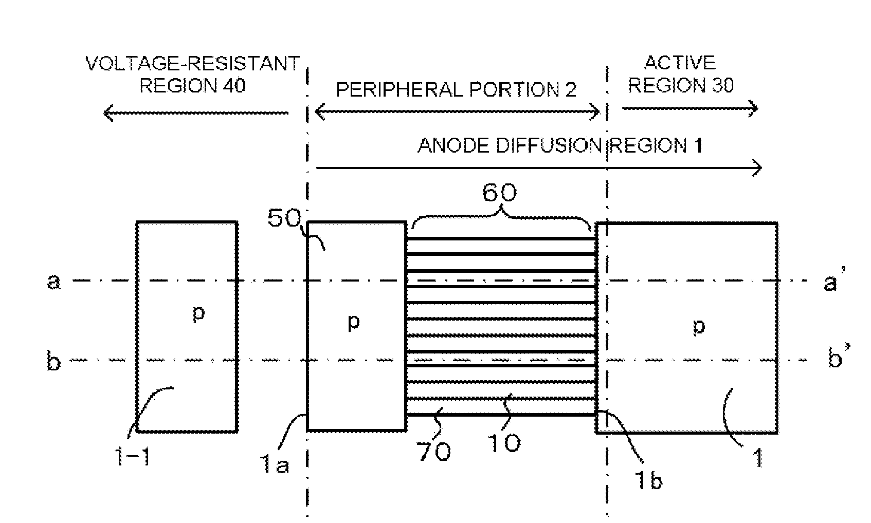
[0055]FIG. 1A is a plan view illustrating main components of a portion of a plane pattern of a peripheral portion of a p type anode diffusion region in a vertical diode as a semiconductor device according to a first embodiment of the invention; FIG. 1B is a cross-sectional view illustrating a surface portion taken along line a-a′ of FIG. 1A; and FIG. 1C is a cross-sectional view illustrating a surface portion taken along line b-b′. FIG. 7 is a plan view illustrating a diode chip according to the first embodiment.

[0056]In the plan view of main components illustrated in FIG. 1A, a peripheral portion 2 which is grown from an outer circumferential end 1b of a p type anode diffusion region 1 has a ladder shape as a plane shape. In other words, a plurality of p type anode stretch-out portions 70 are formed in parallel to each other by stretching out the p type anode diffusion region 1 in a stripe shape from the outer circumferential end 1b of the p type anode diffusion region 1 toward the...

second embodiment

[0069]FIG. 3 is a cross-sectional view illustrating a surface portion of a diode as a semiconductor device according to a second embodiment of the invention. In the embodiment, the peripheral portion 2 of the p type anode diffusion region 1 includes a ladder-shaped extension portion 60 having a short extension width which is substantially equal to the width of the insulating film 3a for insulating the anode electrode 7 and the anode separated electrode 5 (first metal film). In other words, the ladder-shaped extension portion 60 is separated from the p type ring-shaped diffusion region 50 which is connected to the anode separated electrode 5. However, in terms of an electric circuit, the ladder-shaped extension portion 60 and the p type ring-shaped diffusion region 50 are connected to each other through the anode separated electrode 5. In the diode according to the second embodiment, an increase in area of the ladder-shaped extension portion 60 is suppressed, so that it is possible t...

third embodiment

[0070]FIG. 4A is a plan view illustrating a portion of a diode as a semiconductor device according to a third embodiment of the invention; and FIG. 4B is a cross-sectional view taken along line d-d′ of FIG. 4A. In the configuration of the embodiment, the peripheral portion 2 includes the p type ring-shaped diffusion region 50, the stripe-shaped p type anode stretch-out portions 70, and an opening portion 4 which is formed in the insulating film 3, and there is no surface metal film (first metal film 5) which is in ohmic contact illustrated in FIGS. 1A to 1C. According to the configuration, similarly to the first embodiment, in the ladder-shaped extension portion 60, an increase in area of the p type anode diffusion region 1 is suppressed, so that it is possible to increase the sheet resistance. As a result, it is possible to suppress the current density of the current flowing in the ladder-shaped extension portion 60 during the reverse recovery period. In addition, in the exposed po...


PUM


Abstract

A semiconductor device is disclosed. The semiconductor device is capable of obtaining a high reverse recovery resistant amount by allowing sheet resistance of a peripheral portion in a p type diffusion region that is in contact with a metal electrode through an insulating film on a surface to be as high as possible and reducing an increase in cost if possible. The semiconductor device includes: a p type diffusion region that is disposed in a surface layer of the one main surface of an n type semiconductor substrate; and a voltage-resistant region that surrounds the p type diffusion region.

Description

CROSS REFERENCE TO RELATED APPLICATION[0001]The entire disclosure of the inventor's corresponding Japanese patent applications, Serial No. JP PA 2012-115494, filed May 21, 2012, and Serial No. JP PA 2013-006206, filed Jan. 17, 2013, are hereby incorporated by reference.BACKGROUND OF THE INVENTION[0002]1. Field of the Invention[0003]The present invention relates to a semiconductor device such as a power device mounted on a power module or the like, and more particularly, to a semiconductor device having a junction diode structure requiring a high reverse recovery resistant.[0004]2. Description of the Related Art[0005]Recently, as energy saving is desired, power modules used for power converter or the like have been applied to a wide range of fields. For example, as illustrated in FIG. 9, the power module is configured to include a converter unit 100, a brake unit 200, and an inverter unit 300. The inverter unit 300 is configured so that an insulated gate bipolar transistor (IGBT) 301...

Claims


Application Information

Patent Timeline
IPC IPC(8): H01L29/739
CPCH01L29/7393H01L29/402H01L29/404H01L29/7397H01L29/7811H01L29/8611H01L29/0615H01L29/0619H01L29/0634H01L29/0692H01L29/0696H01L29/1095
Inventor KOYAMA, HIROMISHIIGI, TAKASHIFUKUCHI, AKIHIROMOMOTA, SEIJIMATSUI, TOSHIYUKI
Owner FUJI ELECTRIC CO LTD
Why Eureka
Try Eureka