Semiconductor storage device

Active Publication Date: 2015-09-03
RENESAS ELECTRONICS CORP
View PDF0 Cites 2 Cited by
  • Summary
  • Abstract
  • Description
  • Claims
  • Application Information

AI Technical Summary

Benefits of technology

[0010]According to one embodiment, it is possible to reduce a leakage current and suppress a

Problems solved by technology

Therefore, in the resume standby circuit that raises the source potential of the memory cell to be higher than the VSS level disclosed in Japanese Unexamined Patent Application Publication No. 2004-206745, the leakage current cannot be effectively reduced at room temperature.
However, the source potential of the memory cell is at the VSS level in Japanese Unexamined Patent Application Publication No.

Method used


Image

  • Semiconductor storage device
  • Semiconductor storage device
  • Semiconductor storage device

Examples


first embodiment

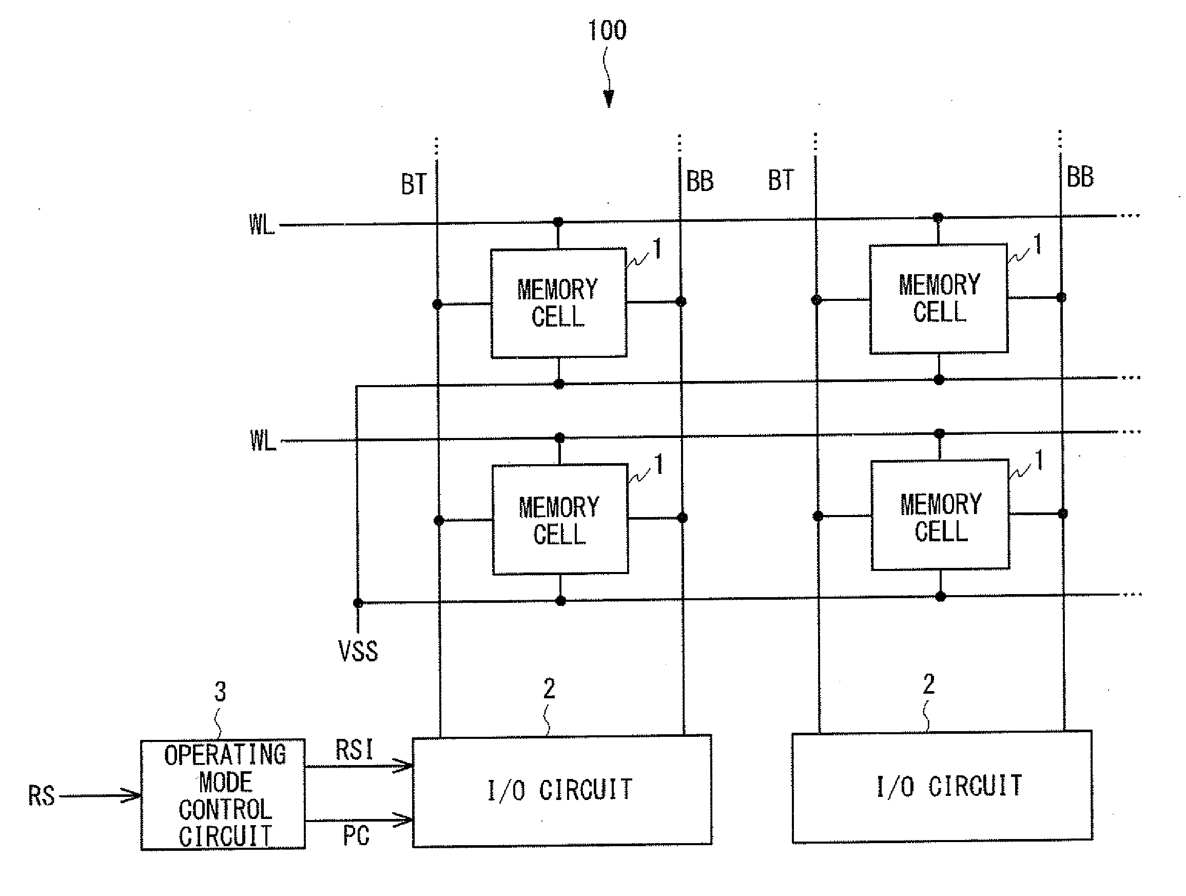
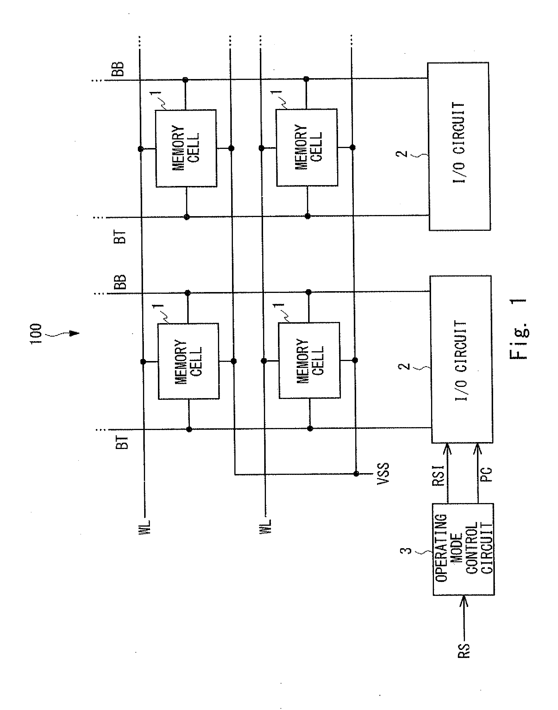
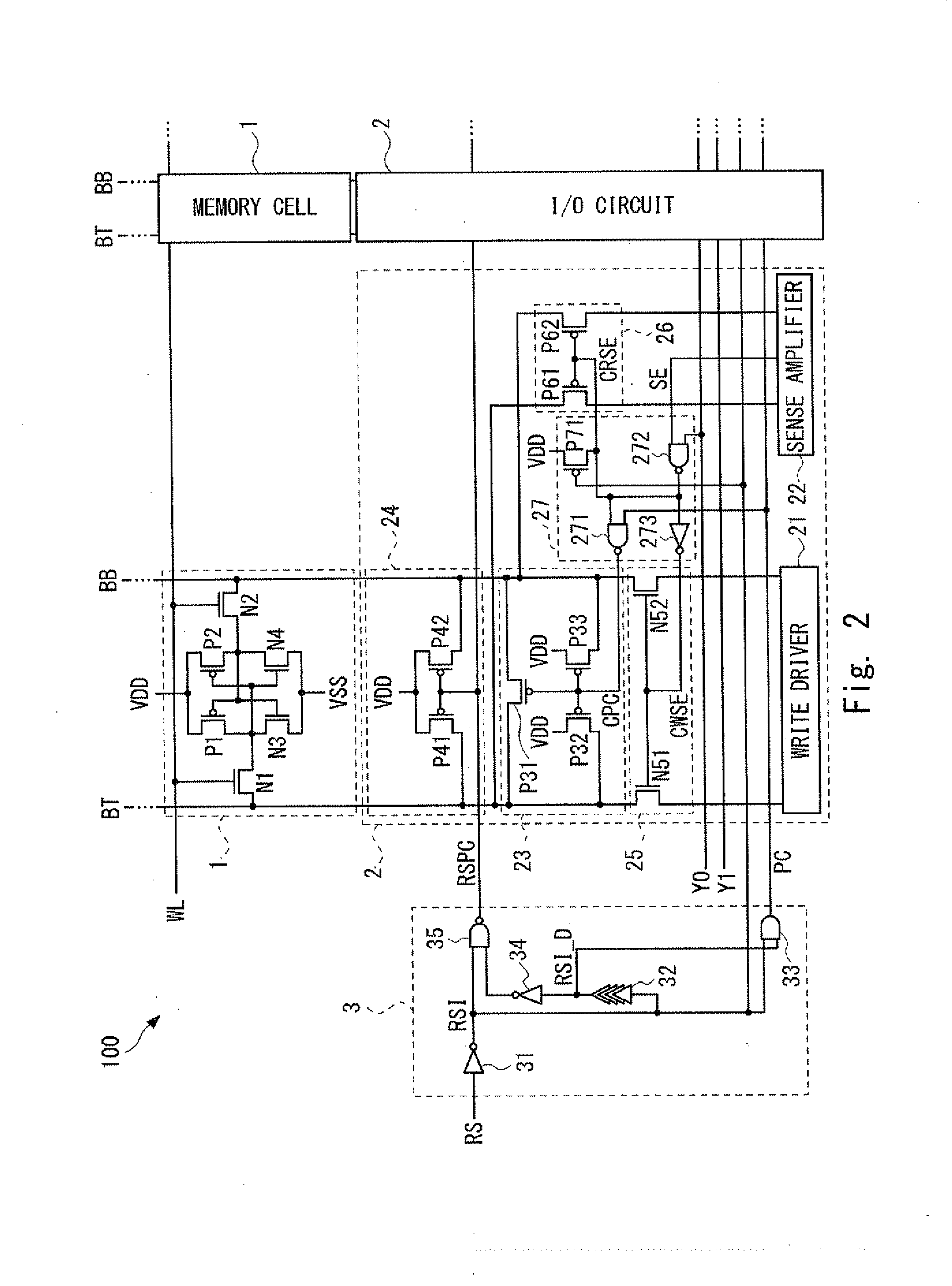
[0024]A semiconductor storage device 100 according to a first embodiment is described hereinafter. FIG. 1 is a block diagram schematically showing a configuration of the semiconductor storage device 100 according to the first embodiment. FIG. 2 is a circuit diagram showing in more detail a configuration of the semiconductor storage device 100 according to the first embodiment. As shown in FIGS. 1 and 2, the semiconductor storage device 100 is configured as SRAM. The semiconductor storage device 100 includes a memory cell 1, an I / O circuit 2, and an operating mode control circuit 3.

[0025]The semiconductor storage device 100 includes a plurality of memory cells, a plurality of word lines, and a plurality of bit line pairs. Note that, however, because the configuration of the memory cells, the word lines and the bit line pairs are respectively the same, each of the plurality of memory cells, the plurality of word lines, and the plurality of bit line pairs is not distinguished from one ...

second embodiment

[0067]A semiconductor storage device 200 according to a second embodiment is described hereinafter. FIG. 5 is a circuit diagram schematically showing a configuration of the semiconductor storage device 200 according to the second embodiment. As shown in FIG. 5, the semiconductor storage device 200 includes a memory cell 1, an I / O circuit 4, and an operating mode control circuit 5.

[0068]The I / O circuit 4 has a configuration in which the resume standby return precharge circuit 24 is eliminated from the I / O circuit 2 described in the first embodiment and further the normal operation precharge circuit 23 and the column I / O control circuit 27 are replaced by a normal operation precharge circuit 43 and the column I / O control circuit 47, respectively. The other configuration of the I / O circuit 4 is the same as that of the I / O circuit 2 and thus not redundantly described.

[0069]The normal operation precharge circuit 43 has a configuration in which the sources of the PMOS transistors P31 and ...

third embodiment

[0081]A semiconductor storage device 300 according to a third embodiment is described hereinafter. FIG. 6 is a block diagram schematically showing a configuration of the semiconductor storage device 300 according to the third embodiment. As shown in FIG. 6, the semiconductor storage device 300 has a configuration in which a word line driver 6 is added to the semiconductor storage device 100.

[0082]FIG. 7 is a circuit diagram showing the word line driver 6 and the memory cell 1 according to the third embodiment. The word line driver 6 includes a control signal generation circuit 61, a driver circuit 62, a resume standby word line holding circuit 63, a return word line power supply switch 64, and a word line power supply switch 65.

[0083]The control signal generation circuit 61 includes inverters 611 to 613, a NOR circuit 614 and a NAND circuit 615. The inverted operating mode switching signal RSI is input to the input terminal of the inverter 611 from the operating mode control circuit...


PUM


Abstract

A semiconductor storage device includes an SRAM memory cell composed of a drive transistor, a transfer transistor and a load transistor, an I/O circuit that is connected to bit lines connected to the memory cell, and an operating mode control circuit that switches an operating mode of the I/O circuit between a resume standby mode and a normal operation mode, wherein the I/O circuit includes a write driver that writes data to bit lines, a sense amplifier that reads data from the bit lines, a first switch inserted between the bit lines and the write driver, a second switch inserted between the bit lines and the sense amplifier, a precharge circuit that precharges the bit lines, and a control circuit that controls the first and second switches and the precharge circuit according to a signal from the operating mode control circuit.

Description

CROSS-REFERENCE TO RELATED APPLICATIONS[0001]This application is based upon and claims the benefit of priority from Japanese patent application No. 2014-040521, filed on Mar. 3, 2014, the disclosure of which is incorporated herein in its entirety by reference.BACKGROUND[0002]The present invention relates to a semiconductor storage device.[0003]In SRAM (Static Random Access Memory), which is one of semiconductor storage devices, various proposals are made for reduction of a leakage current.[0004]For example, a technique that reduces a leakage current by raising the source potential of a memory cell to be higher than the VSS level during SRAM resume standby is proposed (Japanese Unexamined Patent Application Publication No. 2004-206745). In this technique, 0.4V is applied to the source of the memory cell. On the other hand, 1.0V is applied as a power supply potential to bit lines.[0005]Besides, a technique that sets bit lines in floating state during resume standby in order to prevent...

Claims


Application Information

Patent Timeline
IPC IPC(8): G11C11/419G11C5/14
CPCG11C7/12G11C11/419G11C5/148G11C2207/2227G11C7/065G11C7/1057G11C11/412
Inventor ISHII, YUICHIRO
Owner RENESAS ELECTRONICS CORP
Why Eureka
Try Eureka